When a sufficiently high reverse bias is applied to a silicon (Si) pn-junction diode it emits light within a wide spectrum which peaks in the visible range (400<λ<900nm). This basically means that we can observe the light with the naked eye under dark enough ambient, since the relative intensities are quite low. This unique feature of Si is attributed to some high energy electrons (which are accelerated by a high electric field) that recombine with holes after being generated by impact ionization and avalanche. This diode, also called the avalanche-mode light-emitting diode (LED), is a potential light source to enable on-chip optical data-communication in standard CMOS technology. The reason for this is that (1) the light can be detected by a standard Si photodetector in its close vicinity and (2) avalanche is a relatively fast process, which is beneficial for high-speed (~GHz) modulation.
In collaboration with NXP Semiconductors and the integrated circuit design (ICD) group, one of our group members Satadal Dutta has developed a new type of LED called the superjunction LED or in short the SJ-LED (see Fig. 1). This LED comprises a specially designed stack of pn-junctions which are fully depleted prior to avalanche-mode light emission. This full-depletion increases the uniformity of the electric field profile in its active (light emitting) region. Consequently, the area of the light-emitting region is enhanced. Fig. 2 shows some micrographs showing more uniform light emission for the optimized SJ-LED and more localized light spots for a less amount of junctions, within the same device area. The new optimized device showed a ~3 times increased light emission and a 2-fold higher internal quantum efficiency as compared to conventional avalanche-mode LEDs.
The results have been published in the upcoming April 2017 issue (Volume 64, no. 4) of the highly ranked scientific journal IEEE Transactions on Electron Devices.
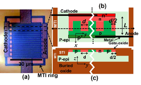
Figure 1 (a) Die micrograph of the SJ-LED realized in NXP’s advanced CMOS technology. The light is emitted vertically (z-axis), (b) Schematic layout of the diode (top view) comprising a multiple amount of parallel pn-junctions (“superjunction”), (c) Schematic cross-section of the diode.
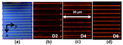
Figure 2 (a) Zoomed-in die micrograph of the SJ-LED. Light emission micrographs (to the same scale) at a fixed current level and integration time with a visible-range camera are shown for (b) an optimized SJ-LED (~40 parallel pn-junctions in a row), (c) an SJ-LED with ~40 parallel pn-junctions in a row, and (d) an SJ-LED with ~20 parallel pn-junctions in a row. Light is emitted vertically (out of plane). Note that the metal lines on the electrodes screen the light.


