Ohmic Contacts to 2D Semiconductors through van der Waals Bonding
Mojtaba Farmanbar and Geert Brocks Advanced Electronic Materials 2, 1500405 (2016).
High contact resistances have blocked the progress of devices based on MX2 (M = Mo, W; X = S, Se, Te) 2D semiconductors. Interface states formed at MX2/metal contacts pin the Fermi level, leading to sizable Schottky barriers for p-type contacts in particular. It is shown that i) one can remove the interface states by covering the metal by a 2D layer, which is van der Waals-bonded to the MX2 layer, and ii) one can choose the buffer layer such that it yields a p-type contact with a zero Schottky barrier height. Possible buffer layers are graphene, a monolayer of h-BN, or an oxide layer with a high electron affinity, such as MoO3. The most elegant solution is a metallic M′X′2 layer with a high work function. A NbS2 monolayer adsorbed on a metal yields a high work function contact, irrespective of the metal, which gives a barrierless contact to all MX2 layers.
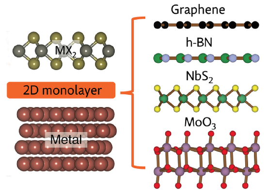
Figure 1. Side view of the metal/buffer/MX2 structure, M = Mo, W, X = S, Se, Te with possible buffer layers graphene, h -BN, NbS2, and MoO3 .


