The research group Inorganic Materials Science of the Faculty Science and Technology of the University of Twente is involved in different aspects of the science and technology of inorganic materials.
The research is focussed on the following activities:
The research is focussed on the following activities:
Animations
- Animations
 Ideal 2D layer by layer growth Under ideal conditions, SrTiO3 can be (homo-epitaxial) grown in a real 2D layer by layer growth: RHEED oscillations.
 Non-ideal 3D growth Non-ideal SrTiO3 growth at lower deposition temperatures: island formation and decrease of RHEED intensity.
 Pulsed laser interval deposition To overcome island growth we suppose pulsed laser interval deposition for induced layer by layer growth. Making use of the high supersaturation during PLD, exact one unit cell layer is deposited with a high laser repetition rate, followed by a period of no deposition. In this case the material is forced to grow in a layer by layer, a unique feature of PLD.
 Deposition of artificial superlattices This is an animation of pulsed laser interval deposition of an artificial YCuO2/BaCuO2 superlattice (i.e. the high temperature superconductor YBaCuO). The in-situ monitoring is done by high-pressure RHEED. After an introduction, you will see in the inset (upper right) the real time RHEED intensity data of the specular spot during the growth of the two different materials and (upper left) simultaneously the HREM image obtained from such a superlattice.
 Growth of SrRuO3 on TiO2 terminated SrTiO3 This is an animation of the growth of SrRuO3 on TiO2 terminated SrTiO3. During the growth a termination shift occurs. After the deposition of 2 unit cells the termination is SrO instead of TiO2. Continuing the growth, a transformation towards step flow growth is observed, depending on the vicinal angle of the SrTiO3 substrate.
TiO2 has green color, SrO is red, and RuO2 is yellow.
 Monitoring PLD with Atomic Force Microscopy We have recently realized a unique system, in which Atomic Force Microscopy (AFM) can be performed during Pulsed Laser Deposition (PLD). With this in-situ AFM island densities and sizes can be measured at deposition conditions.
Chemical materials science & Nanostructured materials
- Chemical materials science & Nanostructured materials
 Development of microporous hybrid membranes Hybrid microporous silica membranes that can be used as an energy efficient separation of small molecules, have still a limited chemical resistance. Doping of the amorphous material with transition metals could solve the prolem.
 Functional oxide nanoparticles Barium titanate (BTO) is used as high-k dielectric phase in multi-layer ceramic capacitors (MLCC).
- Micropattern (large)
 Nanowires and nanocubes During the last couple of years, synthetic procedures for the production of electrochemically synthesized nanowires have been developed in the Inorganic Materials Science lab.
 Self Assembled Monolayers (SAMs) on ultrasmooth metal oxide surfaces Briefly speaking, this project is focusing on Self Assembled Monolayers (SAMs) on ultrasmooth (atomically flat) metal oxide surfaces.
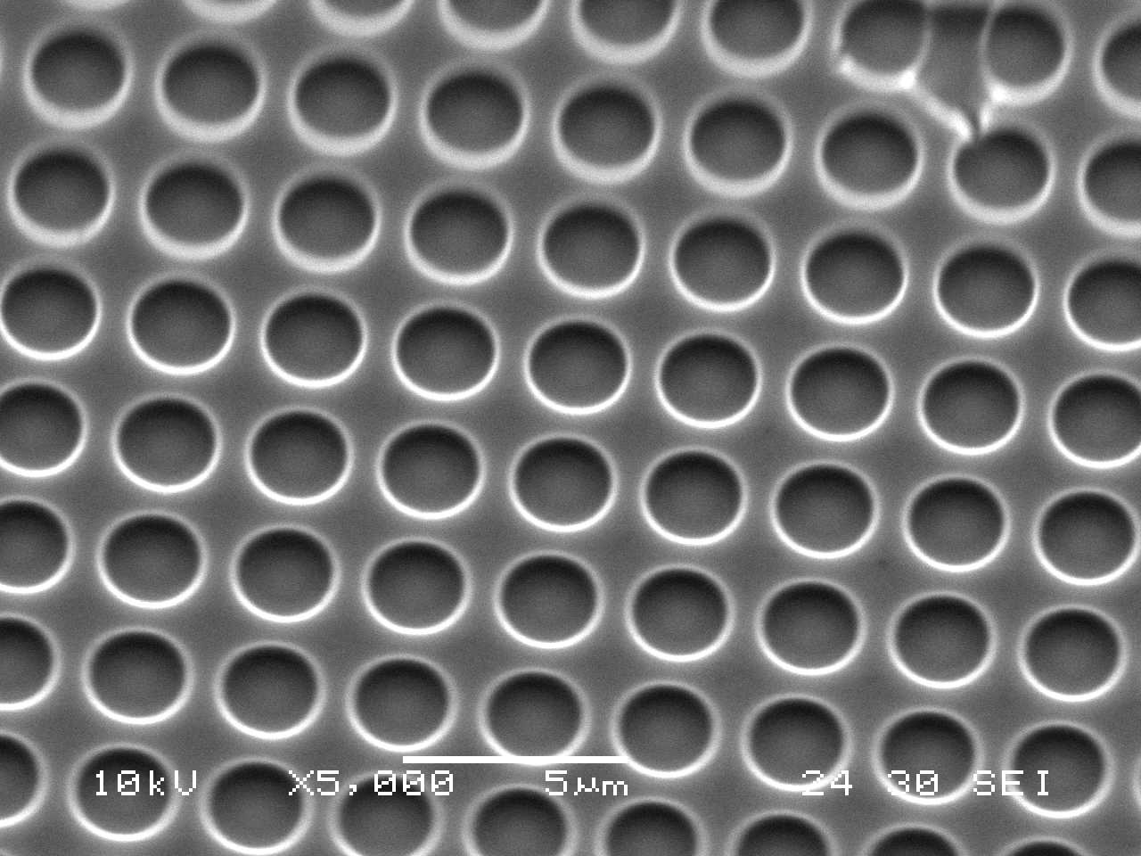
 Soft-lithographic patterning of oxide films The micromolding in channels (MIMIC) technique is used to pattern ceramic suspensions and sol-gel precursors, where the patterns have periodicities typically between 1 and 5 µm.
 Solid state electro-chemistry Several solid inorganic oxide systems show appreciable conductivity for oxygen ions. An important application of this property is found in the so-called Solid Oxide Fuel Cells (SOFCs).
Interface science & Thin film technology
- Interface science & Thin film technology
 Monitoring PLD with Atomic Force Microscopy Currently, in-situ growth morphology characterization is performed by diffraction techniques such as Reflection High Energy Electron Diffraction (RHEED). We have now realized a unique system, in which Atomic Force Microscopy (AFM) can be performed during Pulsed Laser Deposition (PLD).
 Interfaces between complex oxide materials For electrons confined within very small length scales, quantum effects become very important. Quantum wells, structures in which such confinement exists, have been fabricated in semiconductors, which resulted in both better understanding and new applications. The challenge is that the theoretical length scale in complex oxides is much smaller.
 Interface engineering at the La0.67Sr0.33MnO3-SrTiO3 interface After the remarkable discovery of the difference in conductivity of TiO2 and SrO terminated SrTiO3-LaAlO3 interfaces, much attention has been focused on the polar discontinuity driven electronic reconstruction.
Novel devices & applications
 Piezoelectric thin film for energy harvesting device Nowadays, there is a huge requirement in using renewable power supplies, such as batteries. A more efficient and environmental friendly power device is clearly required, instead of using the electrochemical batteries and to lengthen the lifetime of portable electronic device
- Novel devices & applications
 Thin film PiezoMEMS The SmartPie program aims on development of PiezoMEMS (Piezo Micro Electro Mechanical Systems), consisting of all-oxide heteroepitaxial films on silicon substrates.
 Piezoelectric PZT capacitors using metallic SRO electrodes Ferroelectric PZT thin films, due to the low coercive field and high remnant polarization near the morphotropic phase boundary, have been widely investigated for applications in non-volatile random access memory devices.
 Organic single-crystal devices with inorganic dielectrics In this project, molecular organic (pentacene) single-crystal devices (field-effect transistors) with high quality inorganic dielectrics are being studied.
 Thin film O2 and NOx sensors Objective of this project is to investigate and fabricate miniature gas sensors, based on thin films made by PLD. By combining thin film technology with smart sensor designs, we are aiming for low-cost, miniature sensors which can compete with costly, commercially available bulk sensors.
Physical materials science & Artificial materials
- Physical materials science & Artificial materials
 Ferroelectric materials Material science has come to the nano-scale where material properties are dictated by specific atomic structuring and/or combination of materials.
PZT is a well known ferro-electric material which can have, depending on Temperature and Zr/Ti ratio, different structure phases.
 Nonlinear optical properties of materials Besides commonly seen linear optical properties of materials like refraction and absorption, materials respond in a nonlinear way to strong light fields. Growing materials in a particular fashion or making new combinations may lead to such a strong nonlinear response. What materials or designs work best is studied in this research area.