For building quantum computers, making use of both electronics and photonics – technology that works with light – on one and the same chip, is promising. Thanks to silicon technology that we know well from today’s electronic devices, quantum devices could be better protected from influences from the outside world. Another advantage is that they can be scaled up to larger systems. Unfortunately, light and silicon are not the best friends. That is, unless you add germanium to it, in a fully new hexagonal crystal structure. In that case, electronic and photonic quantum bits can indeed be combined. The new European research project ONCHIPS, led by the University of Twente (MESA+/QUANT) in The Netherlands, will work on this ‘best of both worlds’ technology.
Making predictions about the best manufacturing technology for quantum computers is not easy: all approaches have their pro’s and con’s. Some of the quantum bits, qubits, are quite large, need extreme cooling and are very sensitive to their surroundings: there’s only a short time in which you can benefit from their specific quantum properties. Others are more robust and less sensitive to disturbances, but can’t easily be upscaled to hundreds or even thousands of qubits. What you, in fact, would like to do, is benefit from the industrial scale and highly standardized processes used for ‘regular’ semiconductor chips (CMOS). In the combination of silicon and germanium, recently invented, many of the advantages potentially may come together on one chip. This material, having a particular hexagonal crystal structure, was named breakthrough of 2020 by Physics World. The inventors of the material, of the Technical University of Eindhoven in The Netherlands, are a member of the new ONCHIPS consortium.
Energy levels
The hexagonal structure of silicon-germanium has a major advantage: it enables silicon to send and absorb light. In this way, photons can be coupled to electrons that owe their quantum qualities to their ‘spin’: the direction in which they toll around their own axis. This opens whole new possibilities, for example in combining the superior quantum transport properties of photons and the local quantum calculation power of electrons. And all this on the same CMOS electronics chip. One of the problems still to be solved is that creating the hexagonal structure has to be done in an easier way than is feasible right now. What silicon on its own can’t do, and the combination of silicon and germanium can, is associated with the ‘direct band gap’ that is created in this way. An electron can directly cross a barrier between two energy levels, and send out a photon by doing so. Silicon in itself does not have this direct ‘crossing’: the energy levels are not directly above each other, so silicon in itself is not a good light source.
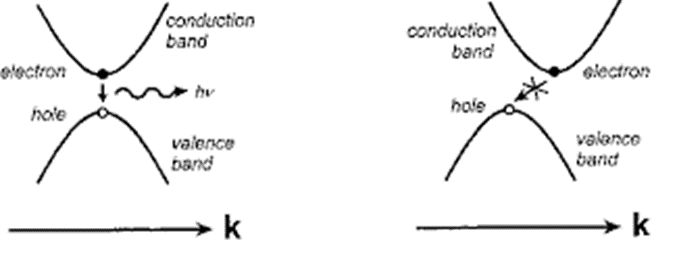
Energy levels, bands, at which an electron can exist. The conduction band is responsible for conducting electric current. Inbetween the conduction band and the valence band, there are forbidden energy levels - the so-called band gap. An electron may cross this bandgap, releasing a photon, in the case of the direct band gap (left). In the situation on the right, the electron can't simply cross because of the indirect band gap.
New materials, new building blocks
 The ‘best of both worlds’ approach may lead to exciting new perspectives in quantum computing, although it is still a challenging task, project leader Professor Floris Zwanenburg says. “Each of our ideas have never been realized in this way. The ambition is understanding more about the best conditions for crystal growth. Furthermore, we have to create the first spin qubits and shape interfaces of these spin qubits and photons. Thorough understanding of the germanium silicon crystal structure is key.” And all that with the future integration of electronics and photonics in mind, on one and the same silicon platform. Zwanenburg leads the ONCHIPS consortium as a member of the Center for Quantum Nanotechnology Twente (QUANT), which is part of the MESA+ Institute of the University of Twente.

 Partners in this new European programme, next to the University of Twente are TU Eindhoven, TU München (Germany), Centre National de la Recherche Scientifique (CNRS, France), Dutch company Single Quantum, Universität Konstanz (Germany) and Budapest University of Technology and Economics (Hungary).


