PROJECT SUMMARY
In recent years considerable progress has been made in making power electronics (PE) such as frequency converters and switched mode power supplies more efficient by using IGBTs (insulate gate bipolair transistor) and switching them faster. Furthermore the voltage swing of IGBTs is higher compared to BJTs. The advantage of IGBTs is that the dissipation is decreased which has a beneficial effect on reliability. The adverse effect is an increased level of electromagnetic interference (EMI); the parasitic capacitance between the transistor and the environment (ground of cool fins) is the current path causing a high level of (mainly) common mode currents. The common mode impedance of the load determines the current amplitude. For instance, in mechatronic and drive applications the parasitic capacitance between the motor windings and the housing closes a common mode loop. The common mode current path cannot be reduced by using feed through capacitances because this will increase the current in the loop formed with the transistor, causing overheating of the transistor.
Thus inductors have to be applied, but these are saturated due to the high level of common mode current. Ferrite inductors become bulky due to the low saturation flux density and the frequency range limited when using steel lamination inductors. The benchmark is that 2 times the volume of the active components is needed for the passive component, and this ratio is still increasing when transistors are switching faster (to reduce heat dissipation within the transistor). Furthermore conventional off-the shelf small and low-parasitic (feed through) capacitors are not available for the large voltage range as applied with IGBTs, especially not for the (ungrounded IT mains supply).
Using an approach in which functional, thermal and electromagnetic effects are taken into account simultaneously, new techniques to solve EMC problems in industrial power conversion systems will be researched and developed. The power electronic functional aspects and the EMC noise aspects will be combined in an integral design approach.
Objectives regarding the performance are:
- reduction in EMI potential;
- reduction in volume;
- reduction in weight while the functional performance and thermal performance remains equal.
In order to achieve the above objectives we will investigate new concepts and innovative techniques. In addition the methods used will be translated into useable design rules for industrial applications, focused on EMI. This will enable industry to design power electronics faster and with lower risk.
Several aspects had been the focus of the research in this project:
- Performance Optimization Aspects of Common mode Filters
- Investigation of the coupling paths of a galvanic isolated AC-AC converter
- Emi Toolkit for frequency converter
- Design of an EMI output filter for Frequency converters
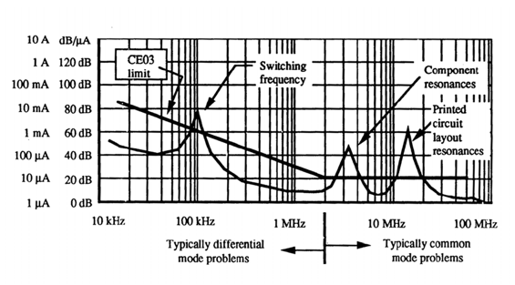
The conducted EMI generates in switching power supply
PERFORMANCE OPTIMIZATION ASPECTS OF COMMON MODE FILTERS
Optimization aspects of common mode chokes are studied. There are based on a behavioral model for common mode chokes and its sensitivity study. Results are used to show the influence of the designable parameters on the final performance of the choke placed in a circuit.
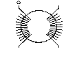
Typical CMC under consideration
Impedances of the CMC
Designable parameters
Zcm
Material (complex permeability)
Dimension of the choke
Number of turns
Effective length
Zdm
Number of turns
Dimensions of the choke
Angle of leakage inductance
Intra Winding Capacitance
And
Turn to Turn
Capacitance
Number of turns
Dimensions of the choke
Wire dimensions and materials(isolation and diameter)
Length of turns
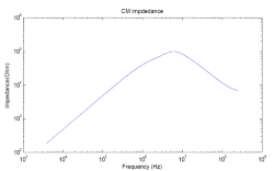
Simulated complex CM impedance of a MnZn sintered core (Dimension: 25*10*5 mm, N=20)
The behavioural model for common mode chokes meets some major requirements: the frequency dependence of the parameters is taken into account to provide accurate results even in higher frequency.
It is also assumed that designers do not have access to a prototype and to experimental values: in addition to electrical information like voltages and currents, others parameters are provided by manufacturers or literature. Small values of parasitics can be integrated in the simulation. The final model is a ‘black box’ for designers. It requires several tested parameters as inputs and provides output needed in graphs and tables. The software Matlab and Simulink have been chosen to develop the presented study.

Topology of the behavioral model for CMC

Impedances of the choke vs. frequency
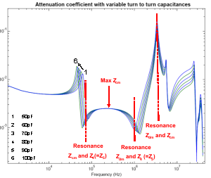
Attenuation coefficient with variable turn to turn capacitances
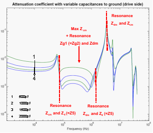
Attenuation coefficient with variable capacitances to ground
![]()
![]()
![]()
![]()
![]()
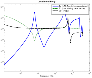
Local sensitivity
Investigation of the coupling paths of a galvanic isolated AC-AC converter
A galvanic isolated three-phase AC/AC converter with a high-frequency AC-link has been analyzed from an EMC point of view. This configuration is novel because of a large number of switches, a high frequency transformer, and a four-wire output. The essential coupling paths are identified. Corresponding suppression remedies are given. The results, before and after measures, are presented to demonstrate the improvement in EMC.
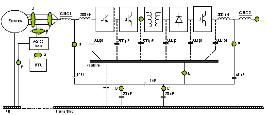
Fig. 3: Equivalent circuit for the common mode current
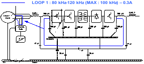
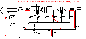
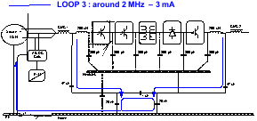
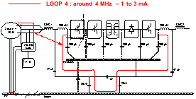
Fig. 5: Main paths of conducted interferences
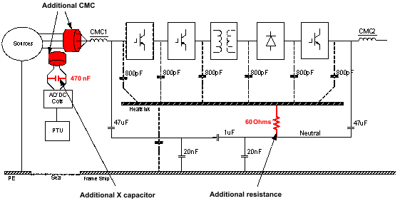
Fig. 8: Final structure of the converter
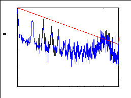
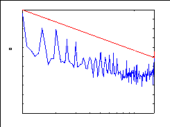
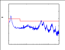
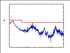
Fig. 2: Initial and final scan of the second phase through the LISN
EMI TOOLKIT FOR FREQUENCY CONVERTER
Picture of the toolkit
Work performs in collaboration with:
- Montage and initial tests: Ye Qiao and Yuefu Qian, Saxion Hogeschool Enschede, The Netherlands
- Emi aspect studies and improvements: Julie Stévovitch and Damien Morisson, ENSIL, Limoges, France
Initial design based on the work of Assoc. Prof. Dr. Werachet Khan-ngern and Mr. Vuttipon Tarateeraseth, supported by the ASEAN-EU UNIVERSITY NETWORK PROGRAMME.
Purpose of the toolkit:
The concept of EMC toolkit is to understand the key conducted EMC issues involving SMPS (switch-mode power supplies), which are composed of a rectifier unit (here a linear power supply) and a DC/DC converter (here a conventional boost converter).
This EMI toolkit permits to study three different aspects: the EMI noise source such as switching phenomena and SRF (self-resonant frequency) of passive device, the control of the EMI effect such as the gate control or the snubber circuit, and the EMI filter which suppresses the CM and DM noises. Moreover this toolkit permits to understand how the EMI can be generated and controlled. Common mode (CM) and differential mode (DM) studies are defined to guide the right concept to achieve the control technique where CM or DM or mixed modes are dominated.
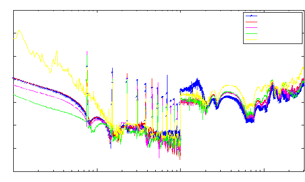
 Some results:
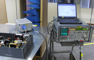
Measurements setup
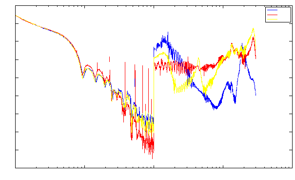
CM current:
Entrance Converter – CM current – Comparison between different EMI filter configurations
Entrance Converter – Comparison between Cy and CMC influence

Entrance Converter – DM current – Comparison between different EMI filter configurations
Entrance Converter – DM current – Comparison between Cy and CMC influence
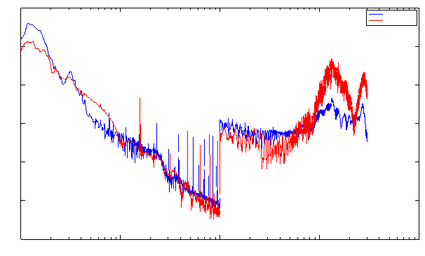
Entrance Converter – DM current – Switch frequency effect
CM current at the output of the input EMI filter – Effect of the common mode choke
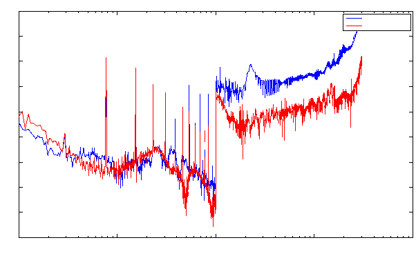
Output of the converter – CM current – Effect of the output EMI Filter
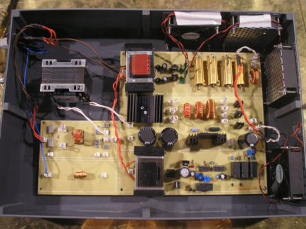
Design of an EMI output filter for Frequency converters
This work has been performed with Hans Bergsma (Thales Nederland, Hengelo in the Netherlands)
A filter has been designed to reduce conducted and radiated emission generated by a frequency converter. The frequency converter, cables and motor were modelled in order to make a good estimation of the radiated emission. A single stage output filter was designed making use of feedthrough capacitors and a nanocrystalline iron particles common mode choke. This choke has a high saturation level, comparable to a conventional iron inductor, and a high permeability, compared to conventional ferrite, i.e. combining the best of both materials. Measurements have shown that such a filter is very effective.
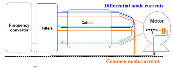
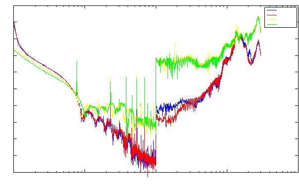
Common mode and differential mode currents at the output of the frequency converter
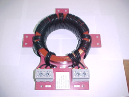
Picture of the common mode choke with nanocrystalline material
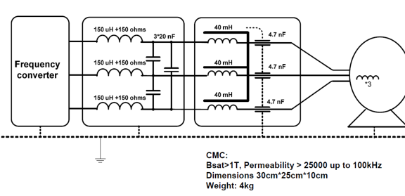
Final structure of the EMI filtering in the motor drive
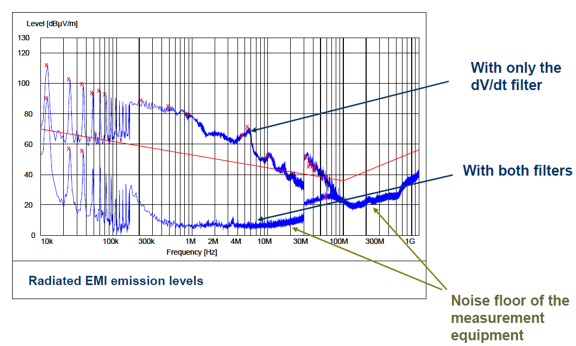
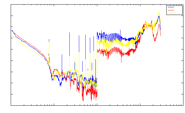
Final performances of the EMI filter.