Novel sensing devices for the IoT era driven by vertical integration
Integration of many different sensing structures with processing electronics in a single chip enables us to realise more versatile and more accurate sensors. Sensors that can - maybe in the future - translate any physical parameter from the real world into digital signal.

Background
I have always been fascinated by physics; the fundamental laws of how the universe works. Especially in an engineering context: how can we use those fundamental laws to realise new things? For a generalist like me, sensors are very interesting, because they translate some real-world parameter (e.g., acceleration, fluid flow or force) into a signal that can be processed by electronics. These devices consist of both mechanical and electrical structures and designing them therefore requires knowledge from different disciplines.
Furthermore, the micro technologies we use to fabricate these miniature devices involve chemistry and a lot of hands-on lab experience too. Designing microfabricated sensors is already a very multidisciplinary process, but integration with smart electronics on a single chip makes it an even more interesting challenge.
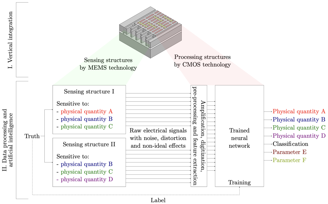
Figure 1 Schematic overview of a sensor integrated with modern processing technologies. Although each sensing structure is sensitive to multiple physical quantities, a value for each quantity can be extracted as long as each sensor’s sensitivities are different.
Novel sensors in the years to come
 Many sensor designers are focused on designing the sensing structures to be as sensitive as possible for one physical quantity. A lot of effort is put into making the sensor robust against unwanted effects, like temperature. But ideal sensors do not exist; physical quantities will always have an influence on the sensing structure.
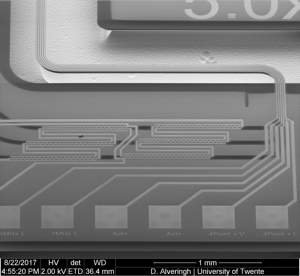
Figure 2 Scanning electron microscopy image of an integrated flow sensor that we have integrated with multiple pressure sensors in the same chip.
Sensor designers are also used to integrate only a few sensing structures in a single chip. More structures require more wires to the electronics (on a different chip) and designers do not really feel the need to integrate more acceleration sensors as there are only three dimensions. In some cases, sensing structures (e.g., MEMS) are integrated with electronics (e.g., CMOS) in the same chip for cost reduction, but this is still limited to a few per device.
We think there is much more potential in this technology as integration helps us to get rid of the wiring issue. It allows us to integrate many different sensing structures, each with a unique set of sensitivities for different physical quantities. Using data processing, the ‘wanted’ signals can be calculated from the many sensor inputs. This requires a lot of (complex) data processing and is ideally performed as close to the sensing structures as possible.
One promising technology that can be realised in the same chip is a neural network that supports deep learning. By exposing the sensor system to each combination of the physical quantities it should be able to measure, the neural network learns how to use its sensing structures to give the desirable output signal. Deep learning can be interpreted as an automatic way to find correlations between sensor outputs and the truth. This means that researchers can also learn a lot from these electronically generated correlations. Or even a step further, novel sensing structures might be (partly) designed by artificial intelligence.
Strange idea? The sensing in our own body works similarly. Many sensory nerves continuously sense forces and temperature on numerous locations in the skin. A brain (neural network) is connected to this chaos of nerves and extracts real-time useful parameters. It can even make decisions: e.g., pull a hand away from a heat source. These nerves have necessarily been wired in a logical way; the hardware is there, but all features have been implemented by learning.
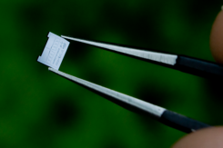
Figure 3 A novel force sensor with a unique combination of high bandwidth and high sensitivity, designed for measuring the impact of microdroplets.
Every parameter in society that is handled by a machine (including computers) must first have been measured by a sensor. Whether it is a complex medical scan or a touch on a keyboard, there is always a sensor between human and machine. This philosophy gives a global impression of the importance of research in sensors for our digital society. Combining sensing structures and a neural network in a single chip is the spot on the horizon; the first steps involve the actual fabrication of such devices.
Education
The multidisciplinary character of microsensors fits very well in the academic technical bachelor and master programmes Electrical Engineering and bachelor programme Advanced Technology. In a first year’s project for example, students learn fundamental physics that are applicable to both electronics and mechanics by designing and building an acceleration sensor. In the master we provide the course “MEMS Design” in which students gain a lot of theoretical knowledge on microfabrication and electromechanical system design.
Collaborations
For our research we work closely with Bronkhorst High-Tech B.V. on the use of artificial intelligence for microfluidic flow and pressure sensing. Furthermore, we are working on large-scale test instruments for MEMS-based sensors in a consortium consisting of Salland Engineering (Europe) B.V., Saxion Hogeschool, MASER Engineering B.V. and Bronkhorst High-Tech B.V.