The SmartPie program within IMS aims on development of PiezoMEMS (Piezo Micro Electro Mechanical Systems), consisting of all-oxide heteroepitaxial films on silicon substrates. Pulsed Laser Deposition will be used to deposit several oxide buffer and functional layers with control of composition, crystalline structure and functional properties.
Piezo technology
Piezo sensors and actuators are widespread in modern society, or example, to open a fuel-valve in diesel engines or to position tools with nanometer accuracy in the wafer steppers for making IC’s. Piezo sensors and actuators are made of ceramic materials, which convert electrical signal into physical displacement and inversely convert the displacement due to an exerted mechanical force into a charge. It was estimated by Nokia that within 5 years, more than 20 piezo elements would be needed in each cell phone, in order to realize all the newly available functions within the smallest possible space.
PZT thin films
PZT thin films are used to develop smaller devices with improved power-efficiency and functionality. Pulsed Laser Deposition is a versatile and fast technique and is capable of tuning the properties of the layers accurately. In general, the properties of highly oriented thin films made by Pulsed Laser Deposition approximate the properties of single crystals. Thin film PiezoMEMS that are developed in this project promise unprecedented compactness and accuracy with respect to current piezo-technology.
Materials Science
Multilayer consisting of the buffer layer yttrium-stabilized zirconia (YSZ), electrodes strontium ruthenate (SrRuO3) and the piezoelectric material PZT are deposited on a silicon wafer. Epitaxy and crystallographic orientation is controlled by a combination of oxide buffer layers between silicon and the functional material. The evolution of the crystallinity is monitored in-situ, using Reflecting High Energy Electron Diffraction (RHEED).
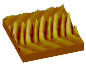
Deformation of a piezoelectric thin film, imaged by Scanning Tunneling Microscopy.
This research will focus on the influence of the crystallographic orientation of the epitaxial multilayers on the functional properties, such as the anisotropic piezo electric coefficients. Furthermore the effect of electrodes on the properties of the device will be investigated.

Electrical characterization of PiezoMEMS device: remanent polarization Pr as a function of the number of switching cycles.
Integrating oxide electronics in silicon technology
A large-area PLD system will be developed, which will allow a scale-up of the fabrication for the PiezoMEMS devices. Incorporating stencil deposition will decrease the number of lithographic steps for patterning the devices.
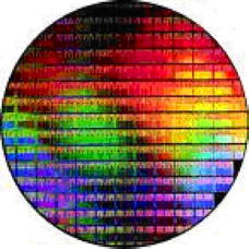
Patterned silicon wafer.
This work is part of the SmartPie program, subsidized through the SmartMix program of ministries of Economic Affairs (EZ) and Education, Culture and Science (OCW). Within the piezoMEMS cluster, we collaborate with C2V and Océ as well as the Transducer Science and Technology (TST) group at the university of Twente.
Within IMS, this research is performed by: Ruud Steenwelle
Daily supervisor: Guus Rijnders