PhD student: Peter de Veen
Daily supervisor: Guus Rijnders
Objective of this project is to fabricate and study molecular organic single-crystal devices (field-effect transistors) with high quality inorganic dielectrics. The original project description can be found here. More background information regarding this project and the latest results can be found below.
Organic Electronics
Since the invention of the transistor in 1947, silicon is still the material of choice for the fabrication of high-performance semiconductor devices. The last decades, however, the field of organic electronics has gained considerable interest. In organic electronics, one or more (or all) inorganic components in a device are replaced by organic materials. The first organic field-effect transistor –the fundamental component in electronic devices– is reported in literature in 1987. The use of organic materials to build electronics seems most attractive in the fabrication of low-cost devices, especially when cheap printing techniques can be used on large area and/or flexible substrates. Displays based on OLEDs and organic RFIDs have already made their way into the commercial market. Also much research is performed the last years on organic solar cells and e-paper.
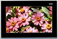
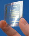
Figure 1 First large diplay (40”) based on Organic LEDs (Seiko) and an organic RFID tag (PolyIC).
Organic semiconductors
Traditionally, the accepted view on organic materials has been that they are not conducting and they are widely used as insulators. In the 1970s, Heeger et al found that polyethylene could become conducting by doping. For this discovery they received the Nobel Prize for chemistry in 2000.
Organic materials with semi-conducting behaviour can be divided as being small-molecular or polymer. Both types have a π-conjugation in their structure. Comparable to CMOS technology, organic semiconductors can be hole conducting (p-type) or electron conducting (n-type). Charge-carrier mobility in electron conducting materials is typically several decades lower than hole conductors, making it still difficult to fabricate complementary devices. Figure 2 shows the typical charge-carrier mobility in inorganic and organic field-effect transistors.
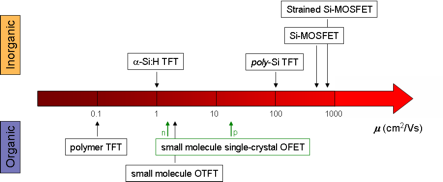
Figure 2 Charge-carrier mobility in inorganic and organic field-effect transistors.
As can be seen in figure 2, charge-carrier mobility in small molecule single-crystal OFETs is one order of magnitude larger than in polycrystalline small molecule OTFTs. The single-crystals, or molecular solids of π-conjugated molecules, are being used to study the intrinsic electronic properties and explore the physical limits of organic semi-conductors. In perfect single-crystals, the electronic properties are not limited by structural defects like grain boundaries. Commercial applications however are not expected to derive from single-crystal devices, as the fabrication techniques for organic thin films are much more promising (thermal evaporation, spin-casting, roll-to-roll and inkjet printing).
Organic Single-Crystal Transistors
Focusing on the fabrication of devices based on organic molecular single-crystals (e.g. pentacene, rubrene) will be the best approach to study the intrinsic electronic properties and to explore the physical limits of organic semi-conducting materials.[1]
In general, two approaches are used in the preparation of devices (field-effect transistors, FET) based on organic single-crystals.[2] Mostly encountered is the ‘flip-crystal’ method, where a single-crystal is simply placed on top of a pre-fabricated source/drain/gate structure, which then ‘bonds’ electrostatically to this structure. However, the nature and quality of the interfaces remain unknown when this method is used. Less encountered is the other approach, where the contacts and gate insulator are deposited directly on top of the crystal surface. With most standard techniques, the deposition damages the crystal surface, thus destroying the interface.
On this project
Objective in our research is to study the electronic transport in the field-effect geometry, i.e. metallic contacts and a gate electrode will be deposited on the organic single-crystal, electrically isolated by an inorganic dielectric layer (see figure 3).To reach high break down field strength, high quality dielectrics need to be deposited. The challenge is to deposit the various layers on the surface of the fragile organic crystal without destroying the interface. The mobility of the charge carriers in a FET is largely affected by the quality of this inorganic dielectric – organic crystal interface.
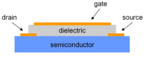
Figure 3 Top-contact FET device.
Pulsed Laser Deposition with stencils
As has been shown in our group, the use of stencils as shadow masks within Pulsed Laser Deposition (PLD) enables controlled deposition of nano to micro structures. The kinetic energy of the arriving species can be controlled by careful parameter selection, which is important for deposition on organic materials. We applied this direct patterning technique to deposit Au and other metallic contacts on an organic self-assembled monolayer (SAM), without destroying the SAM.[3,4] Our intention is to use this method in this research, enabling controlled deposition of structures directly on the fragile crystals (see figure 4).
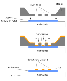
Figure 4 Pulsed Laser Stencil Deposition on Pentacene Single-Crystals.
Experimental Results
First results show that we can deposit and pattern 5-100 micrometer features with a height up to 100 nm of metallic contacts (Au and Pt) and various medium-k inorganic dielectrics (CeO2, Al2O3 and HfO2) on the surface of pentacene single-crystals with this method very controllably. Especially for the inorganic layers very mild deposition parameters are needed to prevent cracking of the deposited film. The fact that the typical pentacene substrate terrace steps (inter-monolayer distance d(001) of 1.41 nm) are still clearly visible on top of the (up to 100 nm high) deposited features indicate a high-quality growth. This enables the fabrication of high-quality top-contact FET devices on organic single-crystals.
References
[1] Reese and Bao, J. Mater. Chem., 16, 2006, 329-333
[2] de Boer, et al., Phys. Stat. Sol. A, 201, 2004, 1302-1331
[3] Speets, et al., Nano Letters, 4, 2004, 841-844
[4] Speets, et al., Adv. Func. Mater. 16, 2006, 1337-1342