
Post Doc
E-mail: l.chang@utwente.nl
Telephone: +31 53 489 3163
Fax: +31 53 489 3511
Address: Faculty of Science and Technology
Medical Cell BioPhysics (MCBP)
Building: Carré
Room: CR4433
Drienerlolaan 5
P.O. Box 217
7500 AE Enschede
The Netherlands
Short Biography
In 2004 Lantian started his undergraduate program, applied physics, in Shandong Normal University, China. After finishing his bachelor in 2008, he decided to focus on Optics.
He pursued his master’s studies in University of Twente (2009-2011) follows the optical track in applied physics. He did his master thesis in Laser Physics and Nonlinear Optics group (LPNO). His master project was to build a continuous wave Optical Parametric Oscillator (OPO) and use that OPO to do absorption spectroscopy of H2 fundamental quadrupole transitions. During his master he grew more and more interest to optical engineering.
He started his first half PhD (2011-2013) in Integrated Optical Microsystem group (IOMS) and continued for the second half (2013-2016) in the Nanobiophysics group in University of Twente. His PhD project was developing a Low-cost handheld optical coherence tomography (OCT) system by using integrate optical waveguide technology. In this project he designed, fabricated and characterized on-chip integrated optical elements (such as microlenses and optical waveguide based power splitters) to replace traditional bulky optical elements (such as mirrors and cube or fiber beam splitters) in an OCT system. This development not only bring down the size (the passive optical parts down to ~100 × 200 μm2) and cost of an OCT system, but also improve the stability of this interference based system. He also developed a parallel OCT system on a single chip which could leads to a faster imaging speed and open up new applications.
Research in MCBP
Integrated Raman FIB-SEM
(Working together with Frank Timmermans on the same project. The following information is from Frank Timmermans.)
Project goals:
Integrating and developing a compact Raman microscope in a Focused Ion Beam – Scanning Electron Beam system. Applications for correlative analysis can be found in the materials and biological sciences, the analysis of plasmonics and multimodal labels will be of immediate general interest.
Integrated Raman FIB-SEM
A Scanning electron microscope (SEM) with a focused ion beam (FIB) enables visualization and material processing with nanometer resolution. The integration of a Raman micro-spectrometer in a FIB-SEM system enables detailed optical spectroscopic material analysis. This provides the opportunity to combine the SEM’s nanometer visual resolution with the Raman microscopes information about the molecular composites. The fully integrated system provides a new tool for comprehensive material analysis. Additionally this system will provide the possibility for material analysis during selected moments of FIB processing on either inorganic materials or biological specimens.
A compact Raman microscope will be integrated with a FIB-SEM system in the MESA+ institute. After integration new developments will be made with the aim of improving the Raman microscopes spatial resolution to decrease the resolution gap between electron microscopy and optical microscopy.
Collaboration:
Hybriscan Technologies b.v.
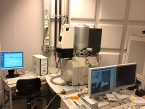
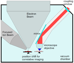
(left) Setup of the integrated Raman FIB – SEM system. (right) A schematic showing the vacuum chamber with incoupling optics for correlative Raman microscopy. The compact Raman microscope is placed outside the vacuum chamber, with only its objective inside.
The next figure shows correlative SEM and Raman images of 1 µm polystyrene beads combined with use of the FIB for site specific ablation. The top images have been taken before and the bottom after the removal with the Focused Ion Beam of the center bead.
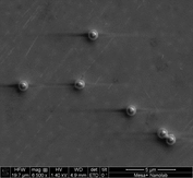
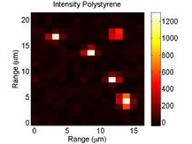
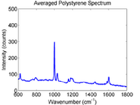

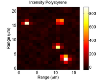
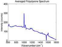
(left) SEM images of 1 µm polystyrene beads. (center) Raman images of the same correlative region. (right) Averaged Raman spectra of the polystyrene signal shown in the center images.