Transparent conductive oxide layers are commonly used in some forms of thin-film PV manufacturing, and in flat panel production. A new project, funded by Solar-Era.Net, is investigating its use in passivated contact crystalline silicon solar cell production. Lennart de Vreede and Thomas Aukes Solmates, a pulsed laser deposition equipment developer located in the Netherlands, outline the project.
In September 2019, the CUSTCO project got to work. The Cost-efficient, Up-scalable and Stable Transparent Conductive Oxides (CUSTCO) group of academic partners include Fraunhofer ISE, the University of Twente, and CNRS LPICM-Ecole Polytechnique. Its industrial partners are Sindlhauser Materials, Indeotec and Solmates. The project’s purpose: to explore how Transparent Conductive Oxides (TCO) can be deployed in passivated contact silicon solar cell production.
Silicon solar cells with full-area passivated contacts have demonstrated efficiencies above 25% in lab-scale research and pilot-line production environments. Such cells are considered one of the most promising pathways toward high-efficiency solar cells. However, full industrialization of these silicon solar cells requires further development and maturation of the associated thin-film processes.
Transparent conductive oxides (TCOs) – which are already widely used in the display industry, touchscreens, and artificial- and virtual-reality applications – are also a key aspect in the performance of several passivated contact silicon solar cell architectures. Since integration aspects between passivating contacts and the TCO materials play a vital role in the performance and stability of such solar cells, the CUSTCO consortium will focus on different combinations of passivating silicon layers and TCO materials. As many different TCO configurations are currently available, the focus of the consortium will be on the evaluation of materials and techniques for the integration of scalable and cost-effective TCO materials with the appropriate silicon contact layers.
The use of amorphous silicon thin films (a-Si:H), microcrystalline silicon oxide (µc-SiOx), and polycrystalline silicon-based (pc-Si) contacts allow investigation of the unexplored potential of TCO materials. An important aspect of this development is the reduction of one of the most widely used elements in TCOs: indium. The scarcity of indium, a rare earth element, limits its suitability in high-volume production applications. The final goal is a demonstration of a cost efficient, scalable and stable TCO deposition technology for a highly efficient (>24%) silicon solar cell.
Pulsed laser deposition
As a result of decades of product development, DC sputtering is at this time the industry standard deposition technology for silicon-based solar cell TCO fabrication and will be addressed by Indeotec within the consortium. Besides standard technologies, there is a focus on novel production methods like pulsed laser deposition (PLD), which is very suitable for both rapid material screening and high-volume manufacturing.
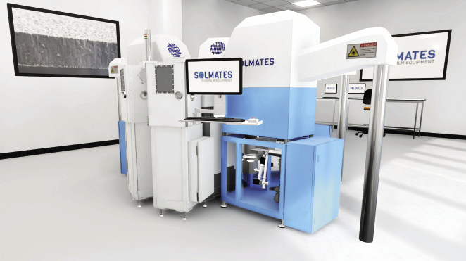
Solmates, based in Enschede, the Netherlands, has developed unique, industrialized PLD platforms that can deposit uniform layers on large areas (up to 300 mm wafers) with low-defect density. Solmates will install such a platform at the University of Twente for TCO evaluation. The key advantages of PLD for TCO processing are high stoichiometric control, room temperature deposition, and control over deposition kinetics to realize a damage-free soft-landing process.
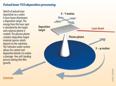 In pulsed laser deposition processing, a target material is illuminated inside a vacuum chamber by a focused UV laser beam to ignite a localized plasma trajectory toward the substrate, as shown in the diagram to the lower left. In order to create uniform layers, both the target and substrate are scanned relative to the stationary laser beam. The thickness of the deposited layer scales linearly with the number of laser pulses and can be controlled with sub-nm resolution. As the laser light interacts with the ceramic target material, small unwanted particles can form which travel with the plasma towards the substrate.
Solmates has developed a unique filtering technology that reduces the number of such particles on the substrate by orders of magnitude, enabling PLD process integration into high-volume manufacturing. Precise control over the kinetics of the plasma during deposition creates the possibility of low damage processing, a key aspect in integration of TCO processes in passivated silicon solar cell designs.
A team lead by M. Morales-Masis at the MESA+ Institute of the University of Twente will use this Solmates large-area PLD system for the development, study and integration of TCO materials in solar cells, including passivated silicon solar cells, in collaboration with Fraunhofer ISE and CNRS LPICM-Ecole Polytechnique.
Lennart de Vreede & Thomas Aukes
About the authors
Lennart de Vreede is a technical account manager at Solmates and the project manager for the CUSTCO initiative. He is passionate about technology and helping others to apply technological advancements.
Thomas Aukes is a technical account manager at Solmates. He holds a master in applied physics. He is a devoted expert on pulsed laser deposition and materials engineering.
The original article can be found below:


