PLASMONIC TUNNEL JUNCTIONS
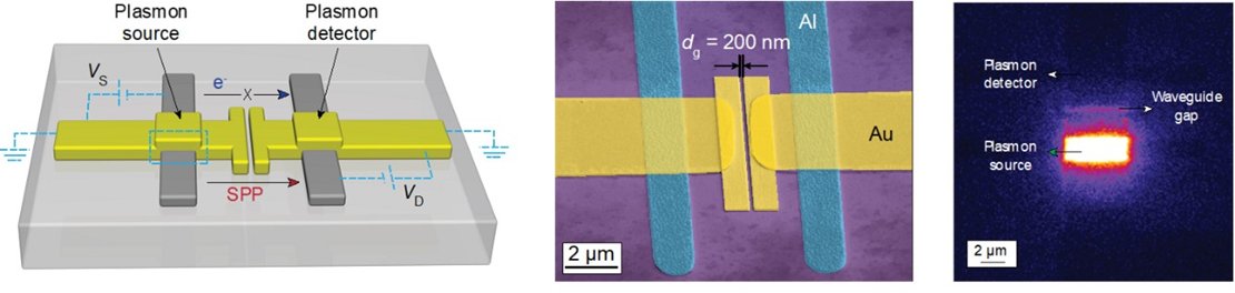
Electrical excitation of surface plasmon polaritons from metal-insulator-metal tunnelling junctions via inelastic tunnelling is interesting from a scientific point of view, and from a practical standpoint for potential applications in nano-optoelectronics. We have developed a plasmonic-electronic transducer based on two Au/AlOx/Al tunnel junctions coupled via a plasmonic waveguide where one junction functions as a plasmon source and the other as a plasmon detector (Nat. Photonics 2017, 11, 623). The figure below shows a schematic of the devices along with a false color SEM image and an EM CCD image of the device in operation where clearly light is emitted from the plasmon source
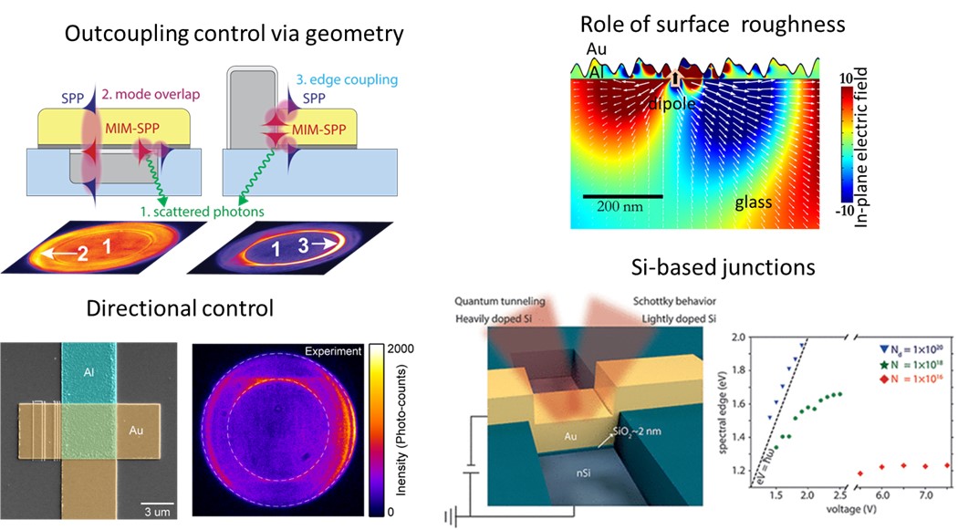
In recent years, we have explored in detail how these junctions work and why they emit light with surprisingly large efficiencies and how the outcoupling of the plasmons can be controlled. We found that surface roughness of the electrodes plays a pivotal role in the outcoupling efficiencies because this roughness provide momentum matching and locally increases the transparency of the electrodes (Adv. Sci. 2020, 190029). In these junctions, first a highly confined mode inside the junction is excited, which then can be outcoupled to all other modes depending on the roughness and geometry of the junction. We found that roughness increases outcoupling efficiencies by orders of magnitude (Phys. Rev. Appl. 2020, 14, 044021), an effect largely underestimated so far. By integrating the junctions with aperiodic gratings we were able to control plasmon propagation direction, and by changing the geometry we could control the outcoupling pathways (Opt. Express 2021, 29, 11987-12000). Recently, we also replace the Au electrodes with Si and demonstrated that in junctions with highly doped Si plasmons can be excited with inelastic tunnelling paving the way for integration with Si-based platforms (ACS Photonics 2021, DOI: acsphotonics.0c01913).