MOLECULAR ELECTRONIC PLASMON SOURCES
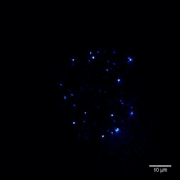
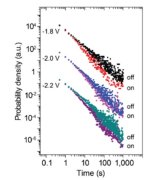
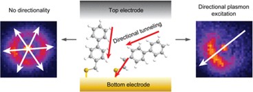
We developed an on-chip plasmon source based on molecular tunnel junctions (Nat.Photon. 2016, 10, 274 – 280). The Figure shows on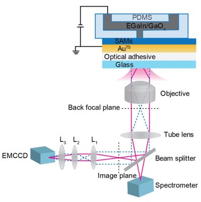 the rights shows a schematic of the SAM-based junctions with the EGaIn top electrode confined in a microfluidic network in contact with a SAM on template-stripped Au. Here, the Au is only about 20 nm thick and therefore semi-transparent making it possible to measure the light emission from the junctions with an inverted microscope platform.The figure below shows that plasmons in these junctions that originate from single, diffraction-limited spots, follow power-law distributed photon statistics, and have well-defined polarization orientations which are controlled by the tunneling direction defined by the tilt angle of the SAM or by simply changing the applied bias of the junction. These junctions excite both localized and propagating SPPs that follow similar blinking statistic as other point sources (such as quantum dots or single molecule emitters (Adv. Sci. 2019, 1900390). The figure below shows the defocused plasmon emission image which indicates the polarization orientation of the plasmon emission spots. Theoretical calculations confirm that the polarization orientation of the plasmon emission can be controlled with the tilt angle of the monolayer (Nano Lett. 2019, 19, 4634-4640).