We are improving our existing methods, and are developing new methods, to form electrical contacts to SAMs electrically. The EGaIn-technique has the advantage that is particularly easy to use in an ordinary research laboratory without the need for elaborate equipment. Here, the metal surface on which the SAMs are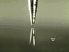 formed serves as the bottom-electrode and the SAM is contacted with a cone-shaped tip of an eutectic alloy of Gallium and Indium (EGaIn) that has a thin, highly conductive surface layer of conductive GaOx of 0.7 nm); this alloy is non-toxic and has non-Newtonian properties so it can be shaped and forms stable features in microchannels (unlike Hg for instance).
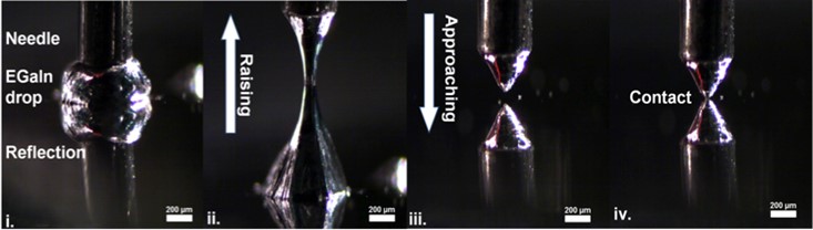
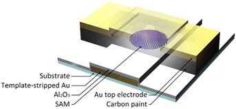
The video and the Figure shows a series of photographs that show (from left to right) the formation of cone-shaped tips of a EGaIn. By just pulling a mico-needle (i) out of a drop of a eutectic alloy of Ga and In (EGaIn away, two head-to-head cone-shaped EGaIn structures can be formed (ii) until the two cones separate. The cone-shaped tip of EGaIn can be brought in contact with the target surface supporting a SAM by simply lowering the microneedle using the same micromanipulator (iii) until contact with the SAM is made (iv). This so-called EGaIn technique was developed in the group of Whitesides, we have expanded this technique and form routinely EGaIn top-electrodes stabilized in microfluidic channels (Adv. Funct. Mater. 2019, 29, 1904452, figure on the left) aligned over micropores making it possible to study the mechanisms of charge transport as a function of temperature, integrate the EGaIn technique with optics, and study the junctions with (potentiodynamic) impedance spectroscopy. We are also exploring methods to replace EGaIn with other materials that are easier to process. The figure on the right below shows a junction with top electrodes of carbon paint that can be readily spincoated onto SAMs (J. Am. Chem. Soc. 2020, 142, 7, 3513–3524).