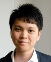
 In this thesis rare-earth-ion-doped amplifiers were studied, being key enabling devices for modern telecommunication systems.
‘Nowadays chip-scale amplifiers are introduced,’ says Yean-Sheng Yong. ‘Rare-earth-ion-doped optical amplifiers are used in long-haul fiber optic communication systems. The use of chip-scale rare-earth-ion-doped material with high active ion concentrations, allows the scaling of amplifier’s device length from several meters down to just several millimetres.’
Yean-Sheng investigated high ytterbium concentration potassium double tungstate waveguide layers, in order to realize small footprint and high gain waveguide amplifiers. The layers are grown on un-doped potassium double tungstate substrates, using cost-effective liquid phase epitaxy techniques.
Spectroscopy properties such as luminescence lifetime, transition cross-sections, and their temperature dependence in high ytterbium concentration waveguide layers, were studied experimentally. New experimental approaches were developed along the way. ‘For example, a novel confocal luminescent lifetime measurement method,’ says Yean-Sheng. ‘This method is non-destructive, does not require additional sample preparation steps, and does not involve extrapolation procedures.’
The experimental methods proved to be applicable in other application devices as well. ‘For example other rare-earth-ion-doped amplifiers or laser materials may benefit. More accurate spectroscopic properties can be found and checked,’ thus Yean Sheng.
During this PhD project, while increasing of ytterbium concentrations – to further miniaturize waveguide amplifiers – new physical phenomena were discovered, such as energy transfer processes and strong temperature dependence of transition cross-sections.
Fundamental issues
‘During early experiments, our measurements didn’t always match our expectations,’ Yean-Sheng shares.
‘When we observed that the wax used to attach our sample on a glass slide melted during an experiment, we decided to focus on these thermal effects more fundamentally. This intersected our previous project plans, turning out our research to become less applied than hoped-for. But that is fine. One has to solve fundamental issues in order to pave the way for high-quality and well performing devices in future. Some indicative results for future devices can be drawn from my work already: not go to the maximum of ytterbium concentrations; and active cooling might result in extra gain.’
Optical lab
Yean-Sheng spent a lot of time working in the optical lab. ‘Now I am used to working in the dark,’ he says.
‘I learnt to build complex experimental set-ups from an empty table, right from scratch. Above that I learnt to find a good balance between performing numerical analyses and setting up new sets of experimental devices and measurements. Also I’m focused more now on learning from experiments in a direct way, so: to learn from what I have really observed! Discussing the observations with colleagues appeared to be very fruitful. The open atmosphere in the Optical Science Group is very favorable for progress in research. I am very grateful for our close collaboration.’
Industrial partners
In this STW funded project Yean-Sheng collaborated with industrial partners, notably XiO Photonics, TE Connectivity, TNO and IBM.
‘The meetings with them were very fruitful,’ he says. ‘As they know the actual working field and the applications requirements better than I do, they were able to inspire us to steer the direction of research in an efficient way.’
skills
Yean-Sheng’s supervisor, Professor Jennifer Herek, encourages him to visit international conferences, and also to attend the meetings of the Applied Nanophotonics cluster within Mesa+.
‘It is interesting to learn about the research projects in other optics groups,’ he says. ‘Now I am going to work as a post-doc, on a device centered around Raman detection. It involves a sensor able to measure, for example, contaminants in water. This work is closer to applications than was my PhD research. I hope to gain extra skills from this project. After that, perhaps an R&D job is within reach for one of the spin-off companies from the University of Twente, for example LioniX. One day I hope to return back to my home country Malaysia and apply my knowledge and skills there.’
QUOTES
When we observed that the wax used to attach our sample on a glass slide melted during an experiment, we decided to focus on these thermal effects more fundamentally.
One has to solve fundamental issues in order to pave the way for high-quality and well performing devices in future.
I learnt to build complex experimental set-ups from an empty table, right from scratch.
Discussing the observations with colleagues appeared to be very fruitful. The open atmosphere in the Optical Science Group is very favorable for progress in research.
One day I hope to return back to my home country Malaysia and apply my knowledge and skills there.
