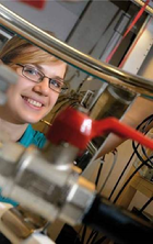
 New unconventional ways to build elements of electrical circuits - like dielectrophoresis, wedging transfer and bottom-up fabrication - were studied and presented in this thesis. ‘We built devices using inorganic/organic components, gold nanorods and nanoparticles in which new self-assembly and inorganic/organic techniques were used,’ Ksenia Makarenko says. ‘We succeeded in measuring fundamental physics phenomena at nanoscale, where classical and quantum behaviour of electrons takes place.’
Mesoscopic physics forms a bridge between the macroscopic world, of bulk materials, and the microscopic world, of atoms and molecules. It explores semiconducting, metallic and superconducting systems with typical dimensions in the range of 0.01-10 μm.
‘In three parallel main fields I investigated fundamental physical phenomena,’ Ksenia Makarenko says. ‘These are: charge transport through a pair of metallic Coulomb islands coupled in parallel; coherent transport through organic molecular monolayers; and dynamical nonlocality in normal metals.’
Device fabrication
Most of these phenomena are hard to explain to a broader audience, Ksenia points out. For example experiments concerning dynamic nonlocality in diffusive systems, where the Aharonov-Bohm effect is used to tune electron transport.
‘One of the central parts of my work is situated around device fabrication,’ she says. ‘I was usually around the top in the Nanoelectronics group when it came to most hours spent working in the cleanroom. That is a funny thing, not very important. But it is a fact: all of my samples were fabricated within the Mesa+ institute, in which I used a wide variety of techniques.’
Top-down and bottom-up
In fundamental mesoscopic research, chemistry plays a crucial role, now and in the future. New top-down and bottom-up techniques prove their promising potential in rapid pace.
Wedging transfer, for example, is a top-down technique which allows soft-contacting of electrodes, covered by self-assembled molecular monolayers without damaging it, leading to 1-2 nanometer wide molecular tunnelling junctions. Ksenia: ‘Wedging transfer is a promising alternative for the fabrication of nano- and micro-sized area molecular junctions, though the necessity for further improvement still exists.’
Nanopil 2.0
Following her defence, Ksenia will be working as a post-doc in the BIOS lab-on-a-chip group, on the renowned Nanopil 2.0 project.
‘Here electrochemical measurements are crucial. I will be able to bring in my expertise in a totally different area of research,’ she says. ‘I expect some biological aspects I have to learn from scratch while working on this project. I will be happy to do so, as I can attribute in a more direct way for the benefits of society.’
Open Days
Apart from using the facilities for fabricating devices and realizing complex experiments – in which professor Wilfred van der Wiel, group members and technicians were of vital importance – Ksenia felt allied to the Mesa+ institute, by attending the Mesa+ Days and the monthly seminars.
Ksenia: ‘Of great importance, in my opinion, are the Mesa+ Open Days for pupils and students from primary and secondary school. I loved to contribute to these events, showing experiments and transferring my passion for research. I hope to inspire pupils to become a researcher one day. In these age groups children are receptive to develop this kind of dreams. During Mesa+ Open Days I am able to show society that academic research is money well-spent.’