Physics of Interfaces and Nanomaterials
Promotion date: September 19.
Promotor: Prof.dr.ir Harold Zandvliet
Assistant promotor: Prof.dr.ir. Bene Poelsema
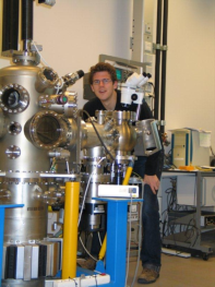
| The main goal was to produce nanowires, with a thickness of one to several atoms, that extend over hundreds of nanometers, produced via the `bottum-up' approach. Physical and electronic properties of these wires can then be studied thoroughly using a Scanning Tunneling Microscope (STM) in ultra-high vacuum conditions. This microscope is capable of imaging surfaces at the atomic level. Furthermore, it can probe the local density of states and can measure dynamics with an excellent time-resolution. Germanium appeared to be a very suitable substrate for this purpose. After depositing Au, Pt or Ir on a clean Ge substrate, and subsequently annealing the substrate to elevated temperatures, perfectly straight and long nanowires were formed. Practical applications of these nanowires could be found in nano-electronics, but also in molecular electronics. Specifically chosen molecules might attach to the nanowire and act as an active electronic component (for example a switch). The Au-induced nanowires showed confinement of electrons in the troughs between the nanowires, thus creating a 1D electron system. Also these nanowires can act as an excellent template for the deposition of molecules for molecular electronic studies. When Co is deposited on Ge it self-organizes into two different types of nanocrystals showing metallic behavior. Also on top of these nanocrystals1D structures were observed. Lastly, electron standing waves patterns in self-organized metallic Ir nanowires on Ge, were visualized. The conduction electrons, i.e. the electrons near the Fermi level, were confined between both ends of the nanowire leading to the observation of electron standing waves patterns and the quantization of nanowire lengths. The growth of Ir nanowires was stabilized by an electronic effect. |
Was your research application driven or more fundamental in orientation?
As Moore’s Law states, miniaturisation in electronics is still taking place for example in smart phone microprocessors. In order to obtain as much efficiency out of these mobile devices, nanowires are the most efficient carriers thinkable. However, quantum phenomena then arise, leading to unthought-of characteristics, like unexpected behaviour of electrons in ‘metal nanowires’. Growing specific chosen molecules on germanium might give rise to new active components, for example a switch. Quasi one-dimensional structures are especially worthwhile studying. If structures build up in a self-organized way the atomic wires are the most thin ones imaginable.
Studying the fundamentals was the most important feature of my thesis work, with which I started immediately after finishing my master work on the same topic, also here at University of Twente. So I took off well-prepared, one could say. One nice feature was that we did not succeed in growing iridium (Ir) nanowires at that time. However, during my PhD project we discovered the right procedure to do so. It was very exciting being able to study these nanowires intensely during my thesis project.
Did your work lead to nice publications?
In fact, my master work already did. It gave rise to a comment in Physics Review Letters in which the work and findings were positively judged, and some facets of the work were taken further by several new PhD’s. We were able to publish some follow-up articles, of which one was published in Nature. At the moment we are trying to publish the results on Ir nanowires. The Ir nanowires appear to grow into distinct lengths. There is a strong relation between growth and quantum size effects, and we show that an electronic effect stabilizes the growth of Ir nanowires.
Publications of my work came out in: Surface Science, the Journal of Physical Chemistry C, and in the Nevac magazine.
Also, quite recently, I had the opportunity to orally present my results on the Materials Research Society spring meeting 2013 in San Fransisco. There I also managed to win a 2nd price at the Science-as-Art competition.
In what way did you develop personally, as a researcher and scientist?
I am much more free in finding my own way in research and giving a personal direction to it. While busy, new opportunities arise along the way. Spotting these and working on them independently, led to some nice publications on at least two occasions. My research skills are much more effective now, including the use of experimentation and measuring apparatus, knowing how to use them in order to find the phenomena one is willing to observe.
Also, I learned to collaborate a great deal more. For example, supervising students experimenting with the STM and working together with other PhD’s led to some nice results along the way. Now, I am much more used in taking a confident lead in these processes.
What are your future plans?
After having a very good time in academics, and learning a lot there, I am curious to use my research skills in industry now. As a student I spent some time in industry already. Now, I would like to find out in what way I can contribute there. For instance in bringing new products to the market, or improving products already existent. I guess, another type of pressure and working spirit is involved in industry than in academics. Spin off companies like Demcon and Solmates or companies in Twente, like Thales, Apollo Vredestein, or elsewhere, like ASML, have a technological basis that would fit my ambitions.
What, in your opinion, is important for Mesa+ to stay successful in future?
When abroad, for example in San Francisco, I experienced that Mesa+ is a renowned institution all over the world, as streaming videos of Mesa+ are presented regularly. In my view it is important to be visible on conferences all over the world.