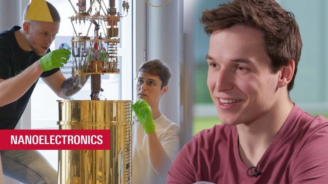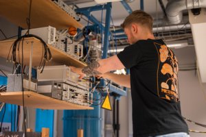
Doing your master or bachelor thesis project at NanoElectronics is possible in several disciplines, such as neuromorphic computing and quantum electronics. In your bachelor or master assignment you will be working on fabrication, characterization and/or modelling of electronic structures on the nanoscale. What will you practically be working on?

Nanofabrication
We fabricate structures at the nanoscale in the cleanroom. The cleanroom offers a dust free environment, with equipment like electron-beam lithography machines and thin-film evaporators, which allow the fabrication of structures of nanometer size.
You will get special training from technicians to work independently in the cleanroom.

Characterization and measurements
After fabricating a sample, you are able to characterize your samples, for example by using low-temperature setups and large magnetic field systems. You have the opportunity to measure at the coolest place of Twente! We have setups that can measure the electronic properties of your device at 300 mK and even at 10 mK in a dilution refrigerator. These cryostats include superconducting magnets with fields going up to 8 Tesla.
Theoretical insights
To understand your experiments it is necessary to relate the results to models. Therefore, application of models, calculations and/or simulations are part of the graduation assignment to understand what is happening in the experiments.
Group members are always willing to support you and to discuss theory and results with you. Furthermore, the group also collaborates with theoretical groups inside and outside the university.
Social activities
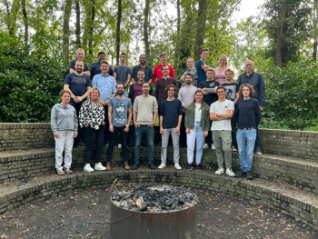
The NanoElectronics Group is a young group with currently about 30 members. Next to science, social events are important in the group. As a student, of course, you are encouraged to take part in daily lunches, coffee breaks, sporting activities, etcetera. Every year there is a NEvent, where you will join the group outing, and have a day of activity and fun.

Interested to graduate in the NE group?
Feel free to contact Wilfred van der Wiel (w.g.vanderwiel@utwente.nl) or Floris Zwanenburg (f.a.zwanenburg@utwente.nl) to discuss the possibilities! Do you want to hear more from a PhD-student about what it is like to be in the group? Contact one of the PhD-students (contact details can be found here).
We provide several courses in the faculties Electrical Engineering, Mathematics and Computer Science (EEMCS), and Science and Technology (TNW). Our group offers:
BSc and MSc thesis projects
Open for students from Applied Physics, Nanotechnology, and Electrical Engineering. The course NanoElectronics (Course code 193400141) is strongly recommended. Further below are the course lists for MSc-EE and MSc-APh students. If you are interested a BSc or MSc project in NE, please read these:
What kind of lab work can I do during my BSc or MSc project?
Which topics can I work on?
As a student in NE you are a full group member and you will be involved in specific aspects of the research, such as device fabrication, measurements and analysis. Besides you are also encouraged to participate in the regular social activities.
The projects listed below give a generic impression of ongoing research. The current situation varies over time, depending on the progress. Please use this list for your initial orientation and selection. After an intake with Floris Zwanenburg you can talk to the PhD students or post-docs to hear more about the status of the projects which have your interest.
HEX- GE/SI NANOWIRES (BSc/MSc)
Supervisors:
Ir. Guido Wiersma (g.wiersma@utwente.nl)
Ir. Romaly Grijpma (r.e.grijpma@utwente.nl)
Dr. Claudius Müller (c.s.a.muller@utwente.nl)
Prof. dr. ir. Floris Zwanenburg (f.a.zwanenburg@utwente.nl)
project:
Semiconductor nanowires offer intrinsically strong confinement in two dimensions, making them an ideal platform to realize spin qubit systems. We explore their fundamental properties, such as the spin-orbit coupling strength, g-factor, and spin decoherence mechanisms. Previous experiments on cubic Ge/Si nanowires [3, 4] have already confirmed their potential.
In this project, the nanowires are made from a novel material, called hexagonal Ge/Si [1]. Due to the hexagonal arrangement of the atoms, the nanowire can efficiently emit and absorb photons [2], unlike cubic Ge/Si. This may solve the problem of long range information exchange, e.g. by forming a “photon data bus” for quantum communication.
Are you interested to help realize spin qubits in novel hexagonal Ge/Si nanowires? Do you want to get to know the ins and outs of nanofabrication? For more information, please do not hesitate to contact us!

References:
[1] A. Li et al., Nanotechnology 34, 015601 (2023).
[2] E.M.T. Fadaly et al., Nature 580, 205–209 (2020).
[3] M. Brauns et al., Appl. Phys. Lett. 109, 143113 (2016).
[4] M. Brauns et al., Phys. Rev. B 94, 041411(R) (2016).
PROBING TOPOLOGICAL SUPERCONDUCTIVITY VIA JOSEPHSON SPECTROSCOPY IN NANOWIRE JUNCTIONS (BSc/MSc)
Supervisor:
Nick Groen
Goal:
In this project, we combine topological materials (SnTe or Cd₃As₂) with a superconductor (Nb) to create topological Josephson junctions. A conventional junction radiates at well-defined frequencies when voltage-biased. By introducing topological elements, we aim to expand this spectrum and reveal the different transport processes occurring within the device.
Students will contribute to the fabrication process from start to finish, conduct ultra-low-temperature measurements, and work hands-on at the frontier of quantum technology.

SINGLE Bi-DONOR ATOMS AS SPIN QUBITS (BSc/MSc)
Supervisors:
Prof. Floris A. Zwanenburg
Dennis van der Bovenkamp,
Mario Simoni
Goal:
Our spin qubit team focuses on exploring new ways of encoding quantum information in solid-state devices. We focus on enhancing the coherence times and fidelities of future quantum computers while deepening our understanding of quantum phenomena at the nanoscale. A key focus area involves investigating the potential of encoding a qubit on the spin of an electron loosely bound to a bismuth donor in silicon. This goal relies on two critical components: a single electron transistor (SET) and a single bismuth atom. We employ the SET as a highly sensitive sensor to detect the variations in the charge states of the bismuth atom. Once a sufficiently strong magnetic field is applied, we can use the SET to sense whether the spin of the bounded electron is in the up or down state. This is a crucial initial step toward functional qubit implementation. Our next generation devices features an on-chip microwave antenna, which will enable us to flip the electron spin states – the final component in creating a fully functional spin qubit.

We fabricate our devices in-house at the MESA+ Nanolab cleanroom, and we test them at cryogenic temperatures in the milli kelvin range, exploiting dedicated equipment (cryogenic fridges, vector magnets) hosted in our laboratory located on the first floor of the Carré building.
Our ongoing research involves:
- Improving fabrication recipe.
- Reducing electrical charge noise in our devices.
- Achieving consistent and reproducible spin readout of the electron bounded to the bismuth atom.
When doing a project in our group, your main focus will be on one of these subjects.

TOPOLOGICAL HYBRID HALL BAR/FET NANOWIRE DEVICES (BSc/MSc)
Supervisors:
Ir. Romaly Grijpma
Goal:
Nanowire-based field-effect transistors (FET) and Hall bar devices are among the most common devices for the material characterization of nanowires. Both geometries can be employed to determine the carrier density and mobility of such nanodevices. However, both types have their advantages and disadvantages. So combined devices are the best of both worlds. It would provide us with a large toolbox which we can employ to observe mesoscopic (magneto)transport features, like Fabry-Pérot oscillations, universal conductance fluctuations or weak antilocalization.
This project would focus on the development of these hybrid device geometries on two types of nanowires. The focus is therefore heavily on nanofabrication, with some electronic transport measurements for characterization of the fabricated devices. Supervision for this project is shared between Femke Witmans and Maarten Kamphuis.
TIME-DEPENDENT PROCESSING WITH RECONFIGURABLE NONLINEAR PROCESSING DEVICES (BSc/MSc)
Supervisor:
Manuel Escudero
Goal:
We are currently studying how Reconfigurable Nonlinear Processing Units (RNPUs) can be combined with dynamic elements (such as capacitors) to create dynamic computational primitives. By embedding temporal behaviour into tunable nonlinear devices, we aim to explore computing schemes capable of processing time-dependent signals. This is a highly exploratory topic with multiple research directions and the potential to contribute to brain-inspired computing architectures. Your project would involve activities ranging from electronic characterization of simple yet not conventional circuits, up to system-level analysis and formulation of
Depending whether you pursue a BSc or MSc assignment, the project can focus on one or more of the following:
- Analysis and modelling of dynamic primitives
- Emergent behaviour through coupling of dynamic primitives
- Using time‑dependent processing in dynamic architectures, e.g., neuromorphic schemes or reservoir computing
NANO EARTHQUAKE MEETS QUANTUM FLATLAND & LEGOS (BSc/MSc)
Supervisors:
Dr. Sourabh Singh
Goal:
A type of electrically controlled nano earthquake on a chip known as Surface Acoustic Wave (SAW) moves along the surface of piezoelectric materials. Concurrently, 2D (van der Waals) materials consist of atomic layers, where electrons are free to move in the plane but shunted along the third dimension. This squeeze, leads to the exhibition of remarkable electronic, optical, and mechanical properties [1]. Interestingly, these atomic layers can also be combined like Lego blocks and new quantum phases can be artificially engineered [2]. SAWs have demonstrated exceptional capabilities in probing and manipulating materials at the nanoscale [3, 4]. The proposed research aims to explore and understand the interaction between SAWs and quantum 2D materials. The goal is to harness this interaction for fundamental studies and subsequently innovative applications.
Projects:
- SAWs will be utilized as non-invasive probe to investigate the magnetic properties of recently discovered 2D ferromagnets. The interaction between SAWs and the magnetic order offers a fascinating avenue for exploration. Traditionally, 2D ferromagnetic materials were associated with low temperatures, requiring extreme conditions to exhibit magnetic behavior. However, CrTe2 has defied this norm by showcasing ferromagnetism at room temperature, a feature that makes it particularly attractive for practical applications. Additionally, its stability at room temperature makes it an attractive candidate for magnetic storage devices, where conventional ferromagnetic materials may face challenges.
- A bound state made up of an electron and a hole is called an exciton. Excitons are quasiparticles in solid-state systems that can be produced using a laser and can also be detected optically. Owing to the bosonic attributes inherent in these entities, excitons offer a more energy-efficient alternative to electrons. Realizing this potential necessitates the development and construction of excitonic circuits capable of transporting excitons in a controlled manner across substantial distances at ambient conditions [2]. SAWs are an excellent contact-free mechanism that can drive the excitons in a controlled direction. In this project, we aim to investigate the transport of room temperature excitons in 2D materials using SAWs.
The assignments will deal with the following aspects:
- Device fabrication in the clean room involving a series of advanced techniques (e.g., electron-beam lithography, optical lithography, evaporation, etc.)
- Optimizing cleanroom processes to develop and fabricate different IDT structures.
- Transferring 2D materials on piezoelectric substrates.
- Collaboration with Physics of interfaces and nanomaterials (PIN) group.
- Microwave measurements using Vector Network Analyzer.
- Develop a fully-coupled finite element micromagnetic method simulation.
- Analyse the simulation results and experimental data to extract key insights into the interaction between SAWs and 2D materials.


References:
[1] Flatland: A Romance of Many Dimensions (Dover Thrift), 1992 by Edwin A. Abbott.
[2] Nature Communications 13, 1334 (2022).
[3] Biosensors and Bioelectronics 237, 115498 (2023).
[4] Phys. Rev. Lett. 130, 246201 (2023).
LOW TEMPERATURE STRUCTURAL PHASE TRANSITION IN SnTe (MSc)
Supervisors:
Ir. Nick Groen
Goal:
Tin telluride (SnTe) is a topological crystalline insulator. This means that it hosts surface states, which are topologically protected by symmetries of the crystal lattice. This implies that deforming the crystal, in other words: breaking the crystal symmetries, affects the topologically protected surface states. SnTe naturally undergoes a structural phase transition at low temperatures.
It is predicted that this structural phase transition induces a spontaneous Hall voltage in the material that can be measured. We want to use this effect to study this phase transition and the effect on the surface states in SnTe, and how this behaviour is affected by alloying the material with lead to form Pb1-xSnxTe.
PROXIMITY INDUCED SUPERCONDUCTIVITY IN PbSnTe NANOWIRES (MSc)
Supervisors:
Ir. Nick Groen
Goal:
Development and optimization of superconducting nanodevices based on selective-area grown nanowires. If we manage to induce superconductivity in these nanowires, we can fabricate all sorts of devices (NIS junctions, Josephson junctions, SQUIDs), that can be used to characterize the topological nature of the quantum states in the system.
This project would include quite a bit of nanofabrication and -optimization, as well as electronic and magnetotransport measurements.
BRAIN-INSPIRED HARDWARE ACCELERATION OF NEURAL NETWORKS (MSc)
Supervisors:
M. Zolfagharinejad MSc (Reza)
Goal:
Brain-inspired computing is a growing and interdisciplinary area of research investigating how the computational principles of the biological brain can be translated into hardware design to achieve improved energy efficiency. Brain-inspired computing encompasses various subfields, including neuromorphic and in-memory computing, that have been shown to outperform traditional digital hardware in executing cognitive tasks. With the rising demand for more powerful yet energy-efficient hardware for large-scale artificial neural networks, brain-inspired computing is emerging as a promising solution for enabling energy-efficient computing and expanding AI to the edge.
Our research focus is to develop new in-materia computing frameworks based on nano-scale dopant-network devices [1]. These recently developed tunable non-linear devices have several electrodes that are used to feed the inputs and tune the desired functionality [2].
One particularly interesting functionality of these devices is the capability of solving non-linearly separable tasks, such as exclusive OR (XOR). XOR can also be solved with a neural network with one hidden layer requiring up to nine operations. Therefore, a single nano-scale device mimics a fully-connected neural network with one hidden layer. This is a great source of motivation toward scaling up the devices into networks of devices to realize large-scale neural networks in hardware [3].

rEFERENCES:
[1] Classification with a disordered dopant-atom network in silicon
T. Chen, J. van Gelder, B. van de Ven, S. Amitonov, B. de Wilde, H.-C. Ruiz-Euler,
H. J. Broersma, P. A. Bobbert, F. A. Zwanenburg, W. G. van der Wiel
Nature 577, 341-345 (2020)
[2] A deep-learning approach to realizing functionality in nanoelectronic devices
Hans-Christian Ruiz Euler, Marcus N. Boon, Jochem T. Wildeboer, Bram van de Ven, Tao Chen, Hajo Broersma, Peter A. Bobbert and Wilfred G. van der Wiel
Nature Nanotechnology 15, 992-998 (2020)
[3] Dopant network processing units as tuneable extreme learning machines
B. van de Ven, U. Alegre-Ibarra, P. J. Lemieszczuk, P. A. Bobbert, H.-C. Ruiz Euler, W. G. van der Wiel
Front. Nanotechnol. 5, 1055527 (2023).
INTEGRATION OF NON-VOLATILE MEMORY IN RECONFIGURABLE NONLINEAR PROCESSING DEVICES
Supervisor:
J. Kareem (MSc)
Project Description
In our group, we work on nanoelectronic devices, in particular on devices called Reconfigurable Nonlinear Processing Units (RNPUs) [1-4]. Our research focuses on their application in machine learning tasks as an alternative computing paradigm, where processing occurs directly within the material itself. This approach aims to move beyond the conventional Von Neumann architecture, which relies on a strict separation between memory and processing, and instead moves toward concepts inspired by the human brain.
The goal of this project is to integrate memory functionality into RNPUs. Specifically, we aim to investigate the incorporation of non-volatile memory elements using ferroelectric materials as well as FLASH memory integrated with RNPUs. The objective is to demonstrate storage or non-volatile memory functionality combined with the intrinsic nonlinear processing capabilities of the RNPU.
The project will involve Technology Computer-Aided Design (TCAD) simulations using Silvaco. You will perform standard semiconductor device simulations to explore and validate the integration concepts. The overall goal is to show that memory and processing functionality can be combined within a single device platform.
Desired Profile
• Completed Mod7A (Device Physics)
• Solid knowledge of fundamental semiconductor device physics
• Willingness to work extensively with TCAD Silvaco simulations, including learning and applying its syntax
Sources
[1] Chen, T. et al. Classification with a disordered dopant-atom network in silicon. Nature 577, 341–345 (2020).
[2] Ruiz Euler, H.-C. et al. A deep-learning approach to realizing functionality in nanoelectronic devices. Nat. Nanotechnol. 15, 992–998 (2020).
[3] Ruiz-Euler, H.-C. et al. Dopant network processing units: towards efficient neural network emulators with high-capacity nanoelectronic nodes. Neuromorphic Comput. Eng. 1, 024002 (2021).
[4] Zolfagharinejad, M. et al. Analogue speech recognition based on physical computing. Nature 645, 886–892 (2025).
Course list Msc Applied Physics
Below the specialization courses:
Strongly recommended for NE:
193400141 NanoElectronics 5
193510040 Theoretical Solid State Physics 5
-Courses in consultation with chair 10
Recommended elective courses:
201600041 Nano-lab: Fabrication & Characterization 5
200900066 Introduction to the Physics of Correlated Electrons 5
193530000 Introduction to Superconductivity 5
193570050 Advanced Quantum Mechanics 5
193400111 Bionanotechnology 5
201600070 Basic Machine Learning 5
201600071 Advanced Machine Learning 5
201700394 Capita Selecta NE
Course list MSc Electrical Engineering
The Chair NanoElectronics (NE) performs research and provides education in the field of nanoelectronics. Nanoelectronics comprises the study of the electronic and magnetic properties of systems with critical dimensions in the nanoregime, i.e. sub ~100 nm. Hybrid inorganic-organic electronics, spin electronics and quantum electronics form important subfields of nanoelectronics. The research goes above and beyond the boundaries of traditional disciplines, synergetically combining aspects of Electrical Engineering, Physics, Chemistry, Materials Science, and Nanotechnology.
Programme mentor: Dr. ir. M.P. de Jong (Michel)
Compulsory courses
Code | Course | Study load (EC) | Quarter |
Materials Science | 5 | 1A | |
NanoElectronics | 5 | 1B | |
Perspectives on Engineering Design | 2,5 | 1B | |
Philosophy of Engineering: Ethics | 2,5 | 1B |
Two additional compulsory courses from the following list:
Code | Course | Study load (EC) | Quarter |
Machine Learning I | 5 | 1A | |
Applied Quantum Mechanics | 5 | 1A | |
Machine Learning II | 5 | 1B | |
Technology | 5 | 1B | |
Integrated Circuit Technology | 5 | 2A | |
Advanced Semiconductor Device Physics | 5 | 2A | |
Semiconductor Project | 5 | Year | |
Nanomaterials Research: Fundamentals, Sysnthesis and Application | 5 |
(Inter)national internships
We have many international contacts to whom we can introduce you, a.o. in Japan, Australia, Switzerland and the USA. If you have done your MSc thesis work in our group then we will happily serve as a reference.
Brain Organoid Electrophysiology
Brain organoid technologies have emerged as a powerful and rapidly evolving in vitro platform for studying complex aspects of human neurobiology, including brain development, neurodegenerative disease, and the emergence of spontaneous electrophysiological activity [1,2]. More recently, they have also enabled the exploration of the concept of organoid intelligence.
Our research focuses on the development and fabrication of advanced electrode architectures for high-fidelity interfacing with brain organoids. These bioelectronic systems are designed to enhance signal quality, spatial resolution, and long-term stability of electrophysiological recordings, while enabling controlled and precise stimulation of neural activity. In parallel, we investigate the underlying electrophysiological principles governing neural communication in these systems. This includes the characterization of signal propagation, network synchronization, and the emergence of functional connectivity in organoid-based neural circuits.
More information: m.o.cicek@utwente.nl
References
[1] R. Kang, S. Park, S. Shin, G. Bak, J. C. Park, BMB Rep. 2024, 57, 311.
[2] A. P. Passaro, S. L. Stice, Front. Neurosci. 2021, 14, 622137.
Courses with a NE contribution
Below is an overview of courses with a NE contribution:
202200177 Electro- and Magnetostatics (BSc EE)
2021100136 Electrodynamics (BSc EE)
201400430 Device Physics (BSc EE)
202000610 Mechanics (BSc AT)
202300118 Error Analysis & Programming Skills (BSc AT)
201700143 Fields and Waves (BSc AT)
201900164 Quantum Matter (BSc AT)
193400141 Nano-Electronics (MSc AP, EE, NT)
191210740 Materials Science (MSc EE, guest lecture)
191210730 Technology (MSc EE, NT, guest lecture)
193400131 Nano-Optics (MSc TN, NT, guest lecture)
191403070 Electromagnetism PM (Pre-master EE, NT)
201900282 Small Signals and Detection (MSc AP)
202001161 and 202001162Graduation Assignment (BSc EE, module 12)
