1.Short overview of research activities
Dave H.A. Blank started his studies on the primary technical school (LTS), followed by the secondary technical school (MTS) and higher technical school (HTS). After his masters in Applied Physics, he received in 1991 his PhD in Physics from the University of Twente, Netherlands for his dissertation on High-Tc thin films prepared by laser ablation: an experimental study, under supervision of prof. dr. Horst Rogalla.
In 1992 he became assistant professor in Rogalla’s group. After a research fellowship at Stanford in the group of prof. Malcolm Beasley and prof. Theodore Geballe in 1998, he was appointed as associate professor and programme director on the materials science of interfaces in the MESA+ Institute for Nanotechnology at the University of Twente. Since October 2002 he is full professor in Inorganic Materials Science at the same university. From January 1, 2007 he is the Scientific Director of MESA+ Institute for Nanotechnology, University of Twente. MESA+ host over 525 scientists and 34 research groups with a total annual budget over M€ 50.
Dave H.A. Blank’s Inorganic Materials Science research group focuses on growth studies, deposition and structuring techniques, and properties of complex materials, especially oxides. The group developed strategies to build, in an atomic layer-by-layer fashion, inorganic materials by true atomic-deposition control and which thereby exhibit novel and unprecedented properties. His research is based in large part on inventing designer-inorganic (tailor-made) nanomaterials that are prepared by atomic precision.
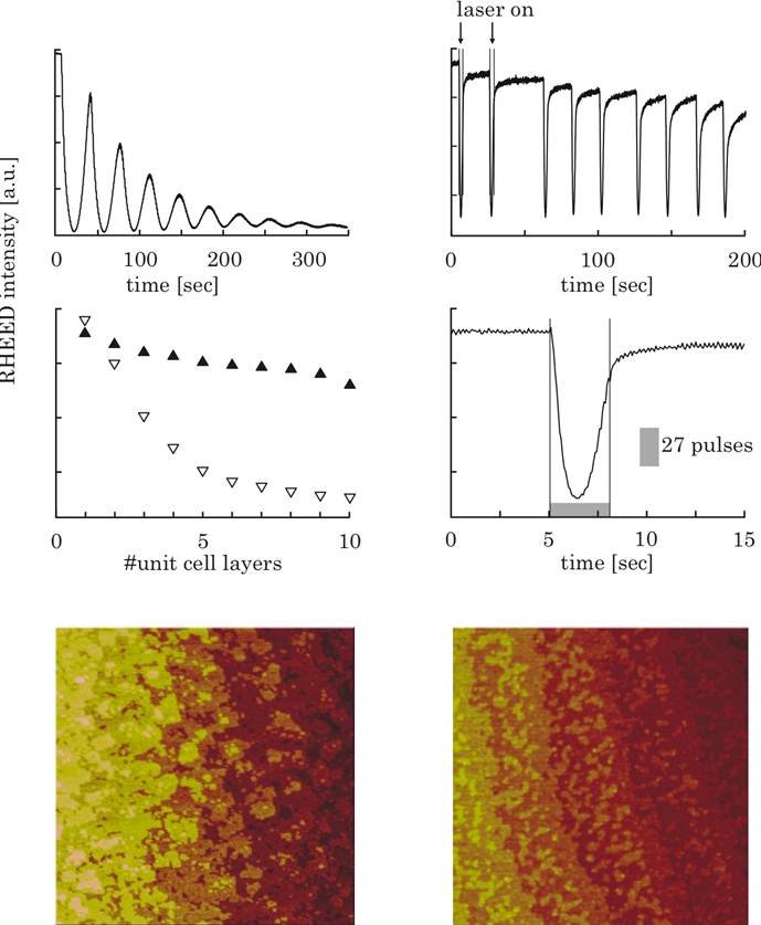
Important development was the first time-resolved high pressure RHEED-system; operating in-situ during pulsed laser deposition at high pressures up to 100 Pa, which he developed together with prof. Guus Rijnders. With this system several new growth phenomena have been observed, leading to new growth techniques of complex materials, like pulsed laser interval deposition. Furthermore, the systems can be used to study and realize block-by-block deposition of (artificial) complex materials. The latter has helped to create an entire new branch of science in inorganic materials which rests on the exact and precise control of atomic arrangements through building structures in a bottom-up fashion and having direct one-to-one, atomic-scale control of the constituting layers.
Overview of Blank’s research contributions in several areas:
High pressure RHEED
A very important innovative contribution is the design and realization of the high pressure RHEED-system operating in-situ during pulsed laser deposition at high pressures up to 100 Pa (Appl. Phys. Lett. 70 (1997) 1888). High pressure RHEED is considered as a breakthrough in thin film deposition with pulsed laser deposition (PLD). Before the introduction of this in-situ technique, PLD was considered as a working horse for complex materials, but not applicable for multilayers with atomic control of the interface. However, with this system several new growth phenomena have been observed, leading to new growth techniques of complex materials, like pulsed laser interval deposition. Furthermore, the systems can be used to study and realize block-by-block deposition of (artificial) complex materials (Nature 433 (2005) 369).
High Temperature Superconductor
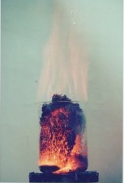
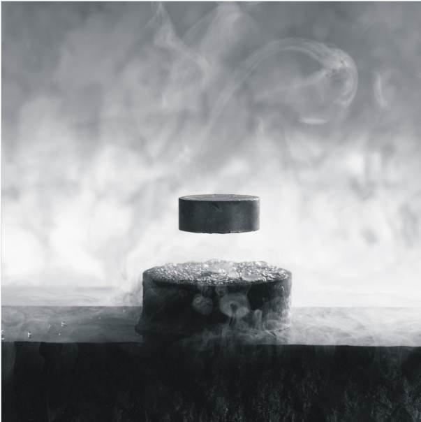
One of his first scientific breakthroughs was the finding of a citrate synthesis of high temperature superconductor YBa2Cu3O7, to date the most pure phase (Journal Physics D 21 (1988) 226). Furthermore, the first high Tc quantum devices (SQUIDs) based on nanostructures was realized (Appl. Phys. Lett. 68 (1996) 1156). After the discovery of superconductivity in MgB2, the first in-situ grown thin films and SQUIDs of the superconductor MgB2 was realized in Blanks group (Appl. Phys. Lett. 79 (2001) 2420). Worth mentioned is the interlayer concept for high transparency contact between superconductors which gave extreme reproducible junctions and exciting physics (Phys. Rev. Lett. 88 (2002) 057004, Appl. Phys. Lett. 80 (2002) 4579, Nature 422 (2003) 50-53).
Growth studies on SrRuO3
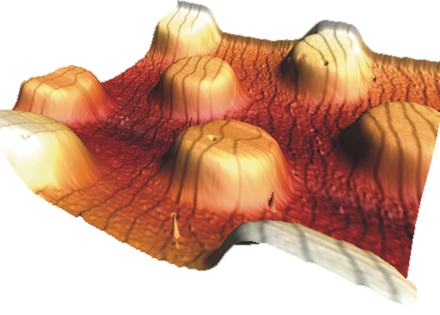
SrRuO3 is one of the most important conducting oxides, used in devices based on (epitaxial) oxide electronics. The growth behavior, from layer by layer toward step-flow growth, of SrTiO3 is very unusual and discussed and explained in detail (Appl. Phys. Lett. 84 (2004) 505, Review Modern Physics (2012) 84 253-298).
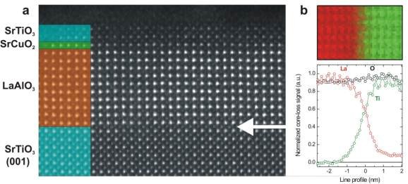
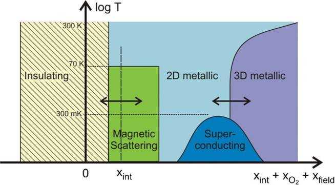
Conducting interfaces
The atomic control of deposition of complex (oxide) systems has introduced the realization of conducting interfaces. Science announced this conducting behavior as one of the breakthroughs of the year 2007 (Science 318 (2007) 1844). Several experiments and discussions has been published on these interfaces (e.g. Nature Materials 5 (2006) 556, Nature Materials 6 (2007) 493, Nature Materials 7 (2008) 270, Adv. Mat. 21 (2009) 1665, Phys. Rev. Lett 104 (2010) 036401, Phys. Rev. Lett. 104 (2010) 166804).
In addition, the realization of fast scanning, high-temperature probe techniques, including probing with nanometre precision could be, as enabling technique, the next breakthrough in growth studies of complex (oxide) materials at the necessary scale of CMOS and MEMS technologies. The Simon Stevin Meester award is used to explore the technique and push it to the limits. Besides growth studies of various materials, the technique will also be used to study organic materials, including viruses, cells and DNA.
Thesis supervisor of the following PhD dissertations
- Wouter Maijenburg “Templated electrodeposition of functional nanostructures: nanowires, nanotubes and nanocubes” (2014)
- Maciej K. Stodolny, “Cr-tolerance of the IT-SOFC La(Ni,Fe)O3 material” (2012)
- Ruud J.A. Steenwelle, “Strain and composition effects in epitaxial PZT thin films” (2012)
- Josée E. Kleibeuker, “Reconstructions at complex oxide interfaces” (2012)
- Antonie George, “Sub-50 nm Scale to Micrometer Scale Soft Lithographic Patterning of Functional Materials” (2011)
- Thomas M. Stawsk, “Understanding Microstructural Properties of Perovskite Ceramics through Their Wet-Chemical Synthesis” (2011)
- Roland Mikkenie, “Materials Development for Commercial Multilayer Ceramic Capacitors” (2011)
- Tian Gang, “Assembly and magneto-electrical characterization of hybrid organic-inorganic systems” (2011)
- Peter de Veen, “Interface engineering for organic electronics. Manufacturing of hybrid inorganic-organic molecular crystal devices” (2011)
- Nicolas Hildenbrand, “Improving the electrolyte-cathode assembly for mt-SOFC” (2011)
- Hans Boschker, “Perovskite oxide heteroepitaxy strain and interface engineering” (2011)
- Michiel Maas, ”Template-electrodeposited nanowires:synthesis, manipulation and application” (2010)
- Oktay Yildirim ”Self-assembled monolayers on metal oxides: applications in nanotechnology” (2010)
- Ming Duc Nguyen, “Ferroelectric and piezoelectric properties of epitaxial PZT films and devices on silicon” (2010)
- Sajid Khan, Soft-lithographic patterning of functional oxide and composite materials2010
- Gerwin Hassink, “Two-dimensional electron layers in perovskite oxides” (2009)
- Paul te Riele, “Direct patterning of oxides by pulsed laser stencil deposition” (2008)
- Wolter Siemons, :”Nanoscale properties of complex oxide films” (2008)
- Joska Broekmaat, “In-situ growth monitoring with scanning force microscopy during pulsed laser deposition” (2008)
- Vittorio Boffa, “Niobia-silica and silica membranes for gas separation” (2008)
- Matthijn Dekkers, “Transparent conducting oxides on polymeric substrates by pulsed laser deposition” (2007)
- Mercy Mathews, “Nanostructures of magnetic oxides” (2007)
- Tijana Zivkovic, "Thin Supported Silica Membranes" (2007)
- Gerald Spijksma, “Modification of zirconium and hafnium alkoxides” (2006)
- Ashima Sah, “Chemically modified ceramic membranes – study of structural and transport properties” (2006)
- Koray Karakaya, “CeO2 and HfO2 high-K dielectrics by pulsed laser deposition: from binary oxides to nanolaminates” (2006)
- Mark Huijben, “Interface Engineering for Oxide Electronics – Tuning electrical properties by atomically controlled growth” (2006)
- Shen Ran, “Ceramic composites of 3Y-TZP doped with CuO: processing, microstructure and tribology” (2006)
- Mai Pham, “Ferroelectric composites of PZT-Pt” (2005)
- Riaan Schmuhl, “Ion Selective Gates – Active device component for 3D microfluidic architecture” (2005)
- Frédéric Mertins, “Perovskite-type ceramic membranes - Partial oxidation of methane in a catalytic membrane reactor” (2005)
- Shankho Roy Chowdhury, “Ordered and disordered porous materials for nanofiltration application” (2005)
- Monse Garcia Curiel, “Polymer-inorganic nanocomposites – Influence of colloidal silica” (2004)
- Dragana Mijatovic, “MgB2 thin films and Josephson devices” (2004)
- Jelena Sekulic-Kuzmanovic, “Porous and microporous titania membranes” (2004)
- Victor Leca, “Heteroepitaxial growth of copper oxide superconductors by pulsed Laser Deposition” (2003)
- Lianne M. Doeswijk, “Pulsed Laser Deposition of Oxides on Silicon: Exploring their Passivation Qualities” (2002)
ThEsis co-supervisor of the following PhD dissertations
- Henk Jan H. Smilde, “Josephson Contacts between High-Tc and Low-Tc Superconductors” (2001)
- Guus Rijnders, “Initial Growth of Complex Oxides: Study and Manipulation” (2001)
- Edward A.F. Span, “Oxygen-Permeable Perovskite Thin Film Membranes by Pulsed Laser Deposition” (2001)
- Gertjan Koster, "Artificially layered oxides by pulsed laser deposition" (1999)
- Boike L. Kropman, "Self-assembly of alkylsiloxane monolayers on perovskite surfaces" (1998)
- Cas A.J. Damen, “Reactive patterning techniques for high-Tc superconductors” (1997)
- Gerard K. van Ancum, “Electronic transport properties of PrBa2Cu3O7-d” (1996)
- Marcel E. Bijlsma , “An in-situ ellipsometric study of high-Tc superconducting thin film growth” (1996)
- Maxim Pedyash, “High-Tc superconducting nanobridges in YBa2Cu3O7 thin films” (1996)
- Bart A.G. Kersten, “Nanostructures on stepped semiconductor surfaces” (1995)