Principal Investigator (PI): Dr. P. Bampoulis
Contact: p.bampoulis@utwente.nl
The Topological Quantum Matter Lab investigates emergent quantum and topological phenomena in low-dimensional materials. We combine low-temperature scanning tunnelling microscopy, conductive and photoconductive atomic force microscopy, nanoscale control, and device-oriented metrology to understand, visualize, and manipulate quantum states in one- and two-dimensional materials. Our goal is to translate fundamental insight into design principles for future low-energy electronic, quantum, and optoelectronic technologies.

The research programme of the lab is organized around three connected research lines.
(1) The first focuses on topological quantum phases and phase transitions in low-dimensional materials, with particular emphasis on germanene. This includes quantum spin Hall physics, one-dimensional topological insulators in ultranarrow germanene nanoribbons, electrically controlled zero-dimensional topological states, and ongoing work toward topological superconductivity, topological field-effect transistors, and correlated one-dimensional phenomena such as Luttinger liquid behaviour and charge-density-wave formation.
(2) The second research line focuses on imaging and control of excitonic and emergent quantum states at the atomic scale in twisted two-dimensional materials. By linking local structure, moiré potentials, defects, and symmetry breaking to electronic and excitonic functionality, we study moiré-confined excitons, defect-bound excitons, and new directions at the intersection of excitonics and topology. In parallel, we are developing holographic imaging with atomic-resolution conductive AFM to probe topological defects and related electronic textures at room temperature.
(3) The third research line addresses the integration and metrology of two-dimensional materials for functional platforms. This includes the stabilization, characterization, and device-relevant integration of low-dimensional materials in collaboration with industrial partners. Current activities span 2D-material architectures for coatings and printing technologies, and defect metrology for 2D materials integrated into silicon-based platforms.
The topological quantum matter lab is supported by competitive national and international funding, including and ERC Starting Grant, NWO Open Competition M1, TKI, and NWO Vidi. The programme is also embedded in broader national and international initiatives such as QUMAT.
The topological quantum matter lab also contributes actively to education and mentorship at the University of Twente through teaching in solid-state physics, nanophysics, and advanced condensed matter physics, and supervision across BSc, MSc levels.
Our current research areas include the following:
Physics of 2D and 1D Topological Insulators
Quantum Spin Hall (QSH) insulators are two-dimensional materials characterized by a bulk bandgap and topologically protected metallic edge states. Theoretical models hint at the potential of QSH edge states to facilitate charge transport without energy loss at room temperature and introduce unique quantum excitations in the form of novel quasiparticles. In this project, we examine germanene, germanene nanoribbons and WTe2 to achieve the following objectives:
- To uncover the principles underpinning charge and spin transport in QSH insulators.
- To identify the quantum mechanisms causing deviations from ideal, dissipationless transport.
- To engineer novel quantum states by controlling electron-electron interactions
- To study topological phase transitions (topological to trivial, 2D to 1D) by controlling their size or applying an electric field.
The Quantum Spin Hall (QSH) effect was predicted for graphene in 2005 by Kane and Mele. This effect relies on spin-orbit coupling (SOC) to form an energy gap in the material's bulk while producing spin-polarized edge states, Figure 1.
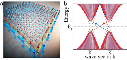
Figure 1. (a) Buckled honeycomb lattice with two sublattices in varying blue shades and the spin-polarized edge states, with red indicating spin-up and blue spin-down channels. (b) QSH insulator band structure with (red shaded area) and without (dashed lines) SOC, depicting the topological gap and the two edge states with red and blue crossing the Fermi level (EF).
Current flowing along these edge states is anticipated to be without dissipation, attributed to time-reversal symmetry and spin-momentum locking. Yet, creating QSH insulators is not straightforward. The tiny SOC in graphene demands temperatures below one Kelvin for the QSH effect to appear, making it unsuitable for many applications. To overcome this, we investigate materials similar to graphene but made out of heavier elements, where SOC is more significant. In this context, Germanene stands out. Germanene is a single layer of germanium atoms arranged in a low-buckled honeycomb lattice. Epitaxial germanene on Ge2Pt(101) is a QSH insulator with a notable topological gap and robust metallic edge states, Figure 2. This sizable gap allows for experiments up to room temperature. The design of Germanene's lattice allows for separate breaking of inversion and time-reversal symmetries. This flexibility facilitates a transition between topological and non-topological phases using for example an electric field. For more details on our work please check our recent publication in Physical Review Letters.
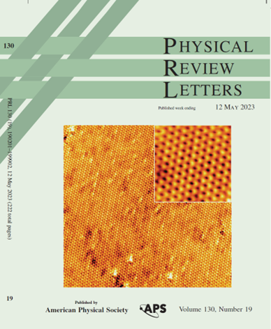
Figure 2. Our recent cover on Physical Review Letters depicting an STM image of the germanene lattice.
By refining the growth process of germanene, we can produce germanene nanoribbon structures that extend over several hundred nanometers and feature straight edges. These ribbons provide a material with a high density of topological edge channels, enabling the study of topological phase transitions. For instance, by reducing the nanoribbon's width to just a nanometer, the nanoribbons could shift from being a 2D topological insulator to a 1D topological insulator.
Topological Field Effect Transistor
Quantum spin Hall (QSH) insulators have an insulating interior, but metallic edges that conduct current without dissipating energy. As a result, these materials have received a great deal of interest for the development of novel low-power electronic and spintronic devices. However, despite their promising features, such devices have yet to be experimentally realized. This project will close this gap by developing a concept topological field-effect transistor, Figure 3, based on the two-dimensional material germanene, that operates at room temperature.
Here, we use our earlier findings (see above) as the foundation of this project to fabricate and scrutinize a room-temperature topological field-effect transistor based on germanene. This revolutionary type of transistor operates by using an electric field to turn ‘ON’ and ‘OFF’ the dissipationless metallic edge channels. In order to achieve our goal, we need to demonstrate that the electronic properties of germanene can be tuned with an electric field at room temperature, and that current flows along the edges of germanene without energy losses. Successful demonstration of a working topological transistor will pave the way for the development of novel low-power electronic and spintronic devices, which could be a potential answer to the increasing challenge of energy wasted in modern computing.

Figure 3. A concept topological field effect transistor device using a 4PP-STM. Two STM tips are used as the source and drain contacts and a third tip as a top gate to switch the topological states On/Off.
Excitons in Transition Metal Dichalcogenides
Transition Metal Dichalcogenides (TMDs) are a class of layered 2D materials with the general formula MX₂, where M represents a transition metal (e.g., Mo, W) and X represents a chalcogen (e.g., S, Se, Te). These materials have garnered significant interest due to their unique optoelectronic properties. Excitons in these materials are electron-hole pairs. Because of the reduced dimensionality and Coulomb interaction in TMDs, these excitons have high binding energies and distinct optical properties. They can be broadly categorized into intralayer excitons (formed by an electron and a hole in the same layer) and interlayer excitons (formed by an electron and a hole in different layers). The spatial separation of interlayer excitons makes them long-lived and gives them unique properties.
Moiré and Interlayer Excitons: When two TMD layers are stacked with a small twist angle, a periodic potential landscape known as a moiré pattern emerges due to the interference between the two atomic lattices. This moiré superlattice potential can trap interlayer excitons, leading to the formation of moiré exciton states. These states can exhibit unique photoluminescence properties, which can be tuned by changing the twist angle.
Defect Bound Excitons: Defects in TMDs, such as vacancies or impurities, can trap excitons, leading to the formation of defect-bound excitons. These excitons have distinct energy levels and can be identified through their unique photoluminescence peaks. Understanding the nature of these defects and their interaction with excitons is crucial for device applications.
Photoconductive Atomic Force Microscopy (pc-AFM) is an advanced AFM technique that measures the local photoconductivity of a material. When combined with optical excitation, pc-AFM can be used to:
- Map the spatial distribution of excitons.
- Identify the origin and nature of defect-bound excitons.
- Investigate the dynamics of interlayer excitons in Moiré superlattices.
By studying the local variations in photoconductivity, pc-AFM can provide insights into the origins and properties of excitons in TMDs. This can be especially useful for understanding the role of defects, interfaces, and stacking configurations on exciton behavior.
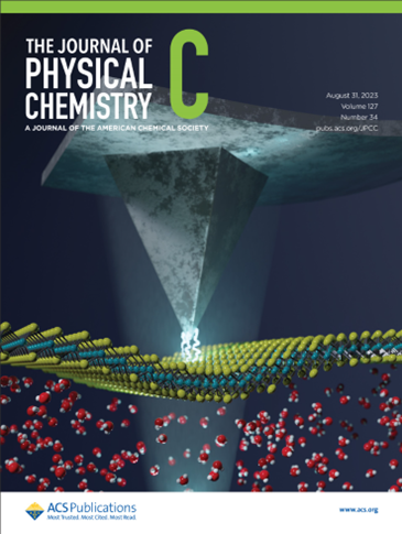
Figure 4. Our recent cover on The Journal of Physical Chemistry C depicting a conductive AFM probe used a probe to measure spatially resolved photocurrents and excitons.
Printing of 2D materials
Comprising a single layer of atoms 2D materials have unique electronic, optical, and mechanical properties distinct from their bulk counterparts. One of the most notable developments in this domain is the ability to "print" these 2D materials, heralding a new era in device fabrication and application. Printing 2D materials is not about traditional ink-on-paper methods. Instead, it is about depositing ultra-thin layers of materials like graphene, transition metal dichalcogenides (TMDs), and hexagonal boron nitride (hBN) onto substrates. Various techniques, such as inkjet printing, roll-to-roll processing, and stamping, have been adapted to handle the unique properties of 2D materials.
The ability to print 2D materials offers numerous advantages: (i) Printable 2D materials can be deposited on a range of substrates, including flexible ones, paving the way for bendable electronics and wearables. (ii) Printing techniques are inherently scalable, allowing for the mass production of devices or coatings with 2D materials. (iii) Printing allows for the precise placement of 2D materials, essential for creating device architectures.
While the promise of printed 2D materials is vast, challenges remain. Ensuring the uniformity and quality of printed layers, integrating with other materials, and scaling production techniques to industrial levels are areas of active research. We are focusing on a novel printing technique in close collaboration with Actega to rapidly advance both materials science and printing technology.