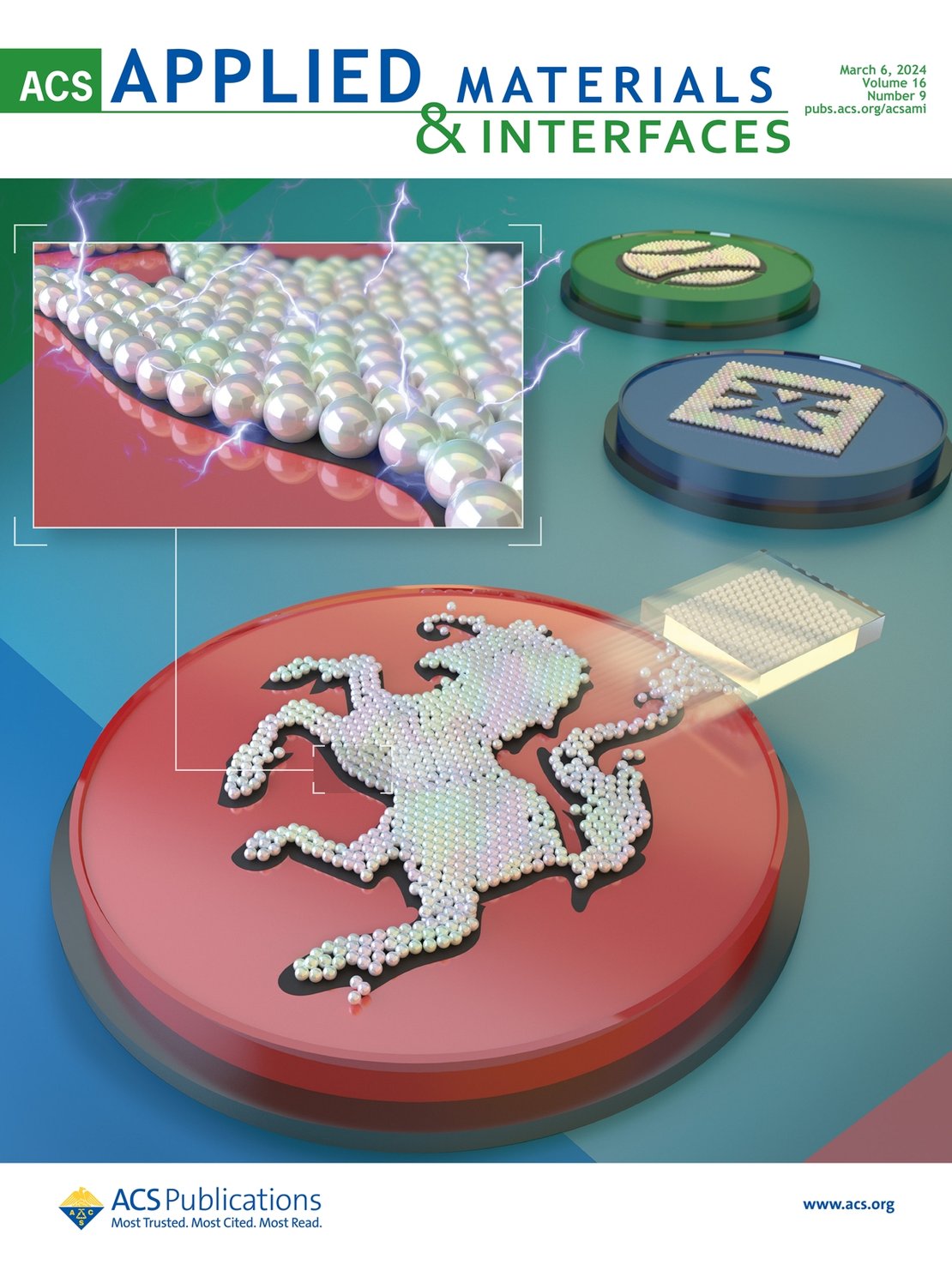
Solvent-free arrangement of nanoparticles for sensors and electronics
Our new article, in collaboration with the VU Brussels and the Riga technical university, appeared on the front cover of ACS Applied Materials and Interfaces. At the bottom of this page you find a video animation of our work.  In this work, we succeeded in arranging nano- and micrometer sized particles in a monolayer without using solvents. To show how much control we have over the process, we created a series of microscopic patterns and logos on a large scale. This is achieved within 20 seconds. The key element in the controlled assembly is triboelectrification, especially on harder surfaces, which is the generation of static electricity by rubbing. We encounter static electricity in every day life, for instance if we rub a balloon against our hair or feel a shock on dry winter day when we touch a metal object. The new assembly method represents a promising development for improving electronics, detecting all kinds of chemical and biological substances, and even detecting counterfeit goods.
Link to the article: https://pubs.acs.org/doi/10.1021/acsami.3c16830
Link to instragram account of the VUB:


