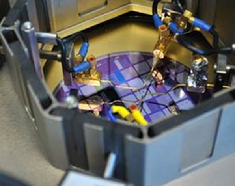
Electrical characterization of devices in microchips is an art in itself. Taking data is easy; getting correct and meaningful information is another thing. We specialize in wafer-level electrical characterization, working with our own devices and materials from Nanolab, but also with industrial samples from R&D or mass production.
For this we share with the Integrated Circuit Design group (ICD) the Measurement Test Centre (MTC) where sophisticated equipment for various types of measurements is available.

Our range of interest includes:
- Current-voltage and capacitance-voltage measurements
- Very high frequency (RF) measurements
- Reliability testing
- Light emission varying from infrared to visible light
- Thermal behaviour of device properties
With the Mesoscale Chemical Systems (MCS) group we share an extensive MEMS test and characterization laboratory, with a.o. a Polytec MSA-600 micro system analyser and a scanning electron microscope. In the MEMS lab we can:
- Investigate vibration modes in micro devices: out-of-plane movements can be detected with picometer resolution; in-plane movements with nanometer resolution.
- Measure topography of micro devices, e.g. measure out-of-plane bending of structures due to stress
- Test and characterize sensors with capacitive readout
- Test and characterize microfluidic devices using a wide range of gases and liquids
