The research focus in this workgroup is on the chemistry and chemical processing of hybrid and inorganic materials and nanostructures, with emphasis on the crystal engineering of metal oxides and layered materials, thin films and low-dimensional nanostructures such as nanoparticles, nanofibers and nanosheets, for applications in the areas of charge storage (batteries & supercapacitors) and thermochemical heat storage.
Electrode materials for Li and Na batteries
Electrodes for batteries are characterized by three elementary properties: (i) charge density (amount of charge per unit weight or volume), (ii) power density (current with which electrode can be charged/discharged), and (iii) cyclability (number of times the electrode can be charged/discharged). In this research theme, we work on the development of new electrode materials that can satisfy these demands and can serve effectively in future generations of batteries. An example of a new phase LixNb18W16O93 as Li anode material, which exhibits an extremely high cycling stability owing to its rigid crystal structure, and a very high power density due to the one-dimensional Li transport channels in the crystal structure, is shown below.
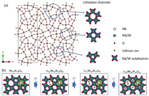
(a) Schematic representation of Nb18W16O93 crystal structure with one-dimensional Li transport channels for fast lithiation/delithiation. (b) Schematic overview of consecutive lithiation steps of the different sites within the lattice during discharge. The full article can be found here.
Other state or the art Li materials currently under investigation are silicon, NMC, and LiFePO4, while layered manganites Nax(Mn,Fe)O2 and related phases are being explored for use in sodium batteries. Most research within this theme is closely liked to and carried out in collaboration with the Nanomaterials for Energy Conversion and Storage work group led by prof. Mark Huijben.
Two-dimensional and layered materials for charge storage
An area of particular interest concerns the use of 2-dimensional oxide nanosheets. Two highly idealized representations of two examples, MnO2 nanosheets of ~0.5 nm thickness (left), and Ca2Nb3O10 nanosheets of ~2.2 nm thickness (right), are shown in the images below.
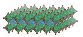
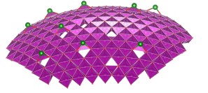
Left: Idealized representation of 2-dimensional calcium niobate nanosheet Ca2Nb3O10 (thickness 2.2 nm). See Right: Representation of part of a MnO2 nanosheet (thickness 0.5 nm) in bent condition, showing Frenkel-type charged surface defects MnIII-vacancy pairs. The full article can be found here.
These nanosheets are essentially 2D nanocrystals that are prepared from a parent layered oxide crystal by a chemical exfoliation process. The resulting nanocrystals can have lateral sizes up to 1-50 mm depending on composition, and since they are so thin they are flexible and can be bent, even though they essentially ionic compounds.
Colloidal solutions of these nanosheets can be deposited into aggregated particles, monolayer coatings or be spraycoated or ink-jet printed into functional materials. The example below illustrates some steps in the process from nanosheet via thin film to functional device.
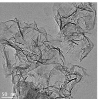
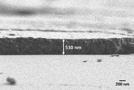
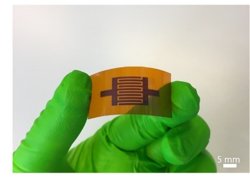
Left: TEM image of MnO2 nanosheets; Middle: Cross-section of printed MnO2 thin film electrode; Right: flexible nanosheet-based thin film supercapacitor. The full articles can be found here and here.
Similar approaches can be used to construct hybrid electrodes encompassing both charge-storing metal oxide nanosheets, and metallic conducting MXenes like Ti3C2. Applications of nanosheets as bulk or thin film electrodes in batteries and supercapacitors are being explored.
For more information, please contact Prof. dr. ir. André ten Elshof.