MSc thesis project
Project Description:
Decades of research on resistive switching epitaxial heterostructures for memory storage have been mostly done on single crystal oxide substrates. However there is a need to explore the possibilities of using silicon in order to move towards more industry-compatible processes. Integrating oxides epitaxially on silicon is a challenging task which involves thermal strain and film-substrate interfacial reactions as additional considerations for growth. The IMS group and other collaborators have worked on buffer layers such as SrTiO3 (STO), yttrium-doped ZrO2, and oxide nanosheets as suitable templates [1]. However for applications requiring conducting electrodes with smooth interfaces free of islands or pinholes, only a limited number of options are currently available.

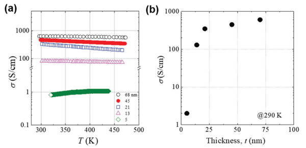
Temperature and thickness dependence of Nb-STO films grown on LSAT substrates. From [2]
Of all the single crystal substrates, STO is the most commonly used. In particular, STO substrates doped with Nb (Nb-STO) at low concentrations (<1%) are the only available conducting perovskite single crystal substrates in the market, however thin films of Nb-STO with the same composition are often poorly conducting. Recently there has been research on pulsed laser deposition (PLD) grown STO doped with higher Nb content which have resistivity values matching those of the single crystal Nb-STO substrates [2]. Integrating the higher doped Nb-STO as a bottom electrode on silicon might make it possible to replicate studies which used Nb-STO substrates as bottom electrodes. Both the Nb-STO and the silicon substrates are sensitive to the oxygen pressure at high temperatures, so the growth conditions must be fine-tuned in order to produce a sufficiently conducting Nb-STO film on silicon.
Project Goal:
Optimize the growth conditions of Nb-STO using PLD in order to obtain sufficiently conducting films which can ideally match the resistivity of the commercially-available Nb-STO substrates.
Role of Student:
The MSc student will learn and use PLD to grow Nb-STO. They will be using substrates of silicon which are already buffered with 4 nm of STO in order to make epitaxial growth of Nb-STO much easier. The effect of the background gas composition, growth pressure, post-growth annealing, etc. will be explored in this study. Furthermore, the student will be doing resistivity measurements with the Physical Properties Measurement System (PPMS), atomic force microscopy (AFM) for surface characterization, X-ray diffraction (XRD) for studying the crystallinity and oxide structure, and X-ray photoelectron spectroscopy (XPS) to obtain the chemical composition of the film.
Contact Information:
Romar Avila (r.a.avila@utwente.nl)
Prof. Gertjan Koster (g.koster@utwente.nl)
References:
[1] B. Chen et al. ACS Applied Materials and Interfaces (2020)
[2] A. Chatterjee et al. Physical Chemistry Chemical Physics (2022)
