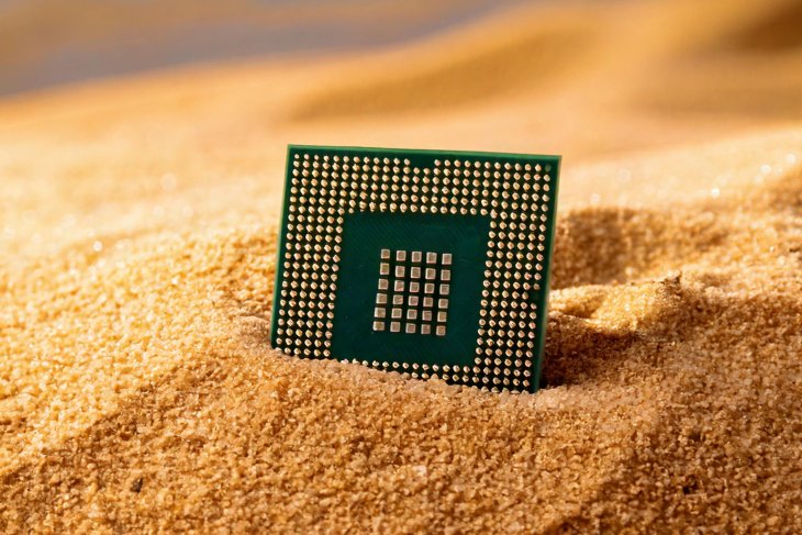
A chip doesn’t come together overnight. It begins with sand and ends with transistors (tiny switches) that are only a few nanometres in size. High-tech equipment is required to craft these intricate, functional works of art. Twente is a pioneer in developing new chip technologies. At the University of Twente, researchers not only create chips but also invent new designs and improve production processes.
How do you make a chip?
Chips are made in a controlled environment known as a cleanroom, like the MESA+ NanoLab at the University of Twente. Temperature, humidity, vibrations, dust, and light are all tightly regulated. A clean room is really clean. In parts of the UT cleanroom, for instance, no more than 29 dust particles larger than 5 micrometres are allowed per cubic metre—compare that with a grain of sand, which is roughly 100 micrometres.
In essence, producing a microchip is done in five steps:
1. Creating wafers
Chips are built on thin, round wafers. usually made of silicon. The silicon needed for the wafer is obtained from a lot of sand. A computer chip is a gigantic network of the smallest circuits. When viewed up close, it resembles a miniature city, complete with roads and buildings.
2. Layering
This ‘city’ is constructed layer by layer. Various materials are applied to the wafer surface, and then shaped into the necessary structures using lithography.
3. Lithography
With the help of lithography, the applied layers are sculpted into the right shape. A light-sensitive layer is evenly spread across the wafer by spinning it at high speed. Then, a specialised machine uses UV lasers to create the design in this layer.
“At the University of Twente, we use an electron beam for this step. While this technique works well on the nanometre scale, it’s too slow for mass production,” says PhD student Reinier Cool. He’s researching ‘brain-inspired computing,’ working on chips designed with the energy efficiency of the human brain in mind.
“Traditional computer chips are essentially powerful calculators, but they consume vast amounts of energy, especially for tasks like AI. For instance, it’s estimated that the human brain uses around 10,000 times less power for similar tasks. Our goal is to create chips that are as energy-efficient as possible for applications like AI, helping to make them more sustainable,” explains Cool.
The laser or electron beam must be extremely precise—just a few nanometres off can ruin the chip. Once the light-sensitive layer is treated, a protective mask remains to guard the next stage: etching.
4. Etch
Unneeded parts of the applied layer are removed with great precision. This etching process reveals the chip’s intricate circuitry. Once complete, the light-sensitive layer is stripped away.
5. Adding conductive material
Silicon alone doesn’t conduct electricity perfectly, so an additional layer of conductive material is added to control the current flow precisely. Lithography is repeated for each layer, applying the conductive material that makes up the chip’s pathways.
6. Pack
In the final step, the individual chips are separated from the wafer with a diamond saw. Each chip is capped with a special cover that includes a coolant to prevent overheating.
These stages are lengthy, with the entire process sometimes stretching over three months. Furthermore, chip technology advances so rapidly that new innovations can surpass designs even before they finish production. There is also a shortage of highly skilled experts needed to design chips and operate these advanced machines. For all these reasons, the global chip shortage is a complex problem with no quick fix.


