Chip technology is the silent force behind many of our modern innovations. From smartphones and internet connections to smart sensors, our connected world would not exist without constant advancements in chip design. At the University of Twente, the Integrated Circuit Design (ICD) research group has been at the forefront of this field for more than 25 years. Their work is not only world-class but has a direct and tangible impact on our daily lives. Here are six groundbreaking innovations that prove this.
1. The Nauta Circuit: A Revolution in Wireless Communication
Researcher: Bram Nauta
It all started in 1987 with an idea while swimming. Bram Nauta – who had just started his PhD research at the time – had an insight that would form the foundation for energy-efficient and fast wireless communication. He quickly left the pool, asked the lifeguard for pen and paper, and sketched a groundbreaking electronic circuit that is now found in nearly all devices.
The so-called Nauta circuit, built from inverters, filters the correct signal from a mix of frequencies. At the time, this resulted in a super-fast chip that was significantly faster and more efficient than existing technologies. Thanks to the Nauta circuit, mobile phones became more energy-efficient, faster in data transfer, and more reliable in signal processing. The design quickly found its way into the telecom industry.
Today, the Nauta circuit is a global standard in smartphones and remains an inspiration for new innovations in chip design.
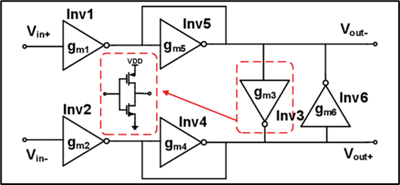
Schematic representation of the Nauta circuit
2. Thermal Noise Cancelling: Less noise, better reception
Researchers: Federico Bruccoleri, Eric Klumperink and Bram Nauta
With the rise of fast mobile internet, smartphones need to receive more and wider frequency bands. This requires broadband receivers, but these have a downside: they generate thermal noise. This noise, caused by heat in electronic circuits, is like a soft static sound that disturbs with reception. The antenna amplifier, which strengthens incoming signals, is the main source of this noise, making it difficult to receive clear signals.
In the 1990s, PhD candidate Federico Bruccoleri, assistant professor Eric Klumperink, and professor Bram Nauta found a solution to this problem. They designed a broadband antenna amplifier that routes the signal through two identical, but oposing paths. This clever technique almost completely filters out the thermal noise, while the desired signal remains intact. The result was an antenna amplifier as sensitive and efficient as narrowband versions but with a much broader application range.
This unpatented innovation is widely used in smartphones today. Based on this principle, it is likely that your phone contains chips. The technique is not only used but also taught in leading textbooks on radio chip design. The research was internationally recognised and awarded the prestigious Jan van Vessem Award for Outstanding European Paper at the ISSCC conference.
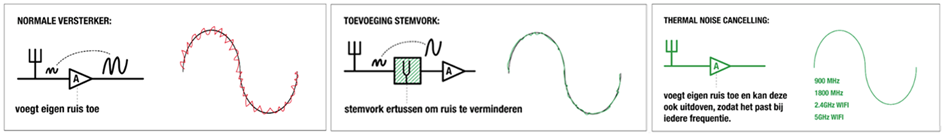
Schematic representation of how Thermal Noise Cancelling works
3. 1/f noise reduction: Precision without interference
Researcher: Arnoud van der Wel
Transistors—the tiny switches that amplify or control signals in almost all electronic devices—naturally produce noise. This noise, a type of background noise, makes very precise measurements difficult. Arnoud van der Wel developed a smart solution: by briefly turning the transistor off and then back on, the noise does not get a change to build up.
You can compare it to a horror film in the cinema. Imagine you want to enjoy the sharp 4K visuals and Dolby surround sound without the scary storyline. By restarting the film every minute, you enjoy the technical quality without letting the storyline—the noise—fully develop.
This technique, known as 1/f noise reduction, is widely used today. It is essential in measurement amplifiers and other applications requiring extremely accurate measurements. Thanks to Van der Wel’s work, electronic systems can now operate with unprecedented precision.
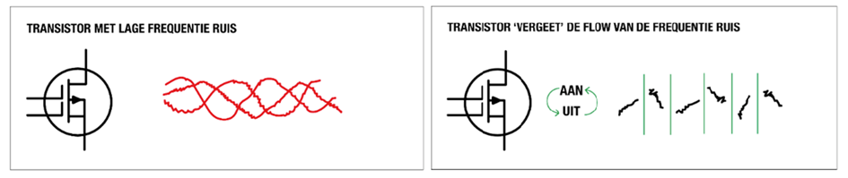
Illustration of 1/f Noise Reduction
4. Subsampling Phase Locked Loop (SSPLL): Efficiency at High Frequencies
Researcher: Xiang Gao
Modern computers and electronic devices process massive amounts of signals that must arrive at precisely the right time. To control this timing, devices use a special circuit called a Phase Locked Loop (PLL). This component ensures that signals stay synchronised, comparable to a well-organised traffic flow.
However, traditional PLLs have two challenges. First, small timing deviations, called jitter, can lead to less accurate performance. Second, correcting these deviations consumes a lot of energy, making the circuit less efficient.
Xiang Gao designed a new technique called Subsampling Phase Locked Loop (SSPLL). This circuit controls and corrects the timing of signals in a much smarter way. As a result, devices perform more accurately and consume less energy. This innovation not only makes technology more efficient but also more sustainable.
Today, Gao’s innovation is used worldwide in computers and other devices. Resulting in better performance and lower energy consumption, which is crucial in a world increasingly dependent on electronics.
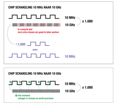
View of Subsampling Phase Locked Loop
5. N-Path Filters: Smaller chips with versatile applications
Researchers: Milad Davishi and Amir Ghaffari
Electronic devices like smartphones, Wi-Fi routers, and Bluetooth devices use filters to process signals. These filters ensure that only the desired frequencies pass through while blocking others. However, traditional filters, especially at high frequencies, can be large and difficult to adjust.
Milad Davishi and Amir Ghaffari developed the innovative N-Path Filter, a technique that uses so-called passive mixers. This technique transforms a low-pass filter – which allows low frequencies to pass through – into a filter that works at higher frequencies. It allows a single filter to adjust to a wide range of frequencies depending on the clock frequency driving it.
You can think of it like a child on a swing. The swing moves back and forth, converting potential energy (when the swing is stationary) into kinetic energy (when the swing is in motion). In an N-Path Filter, something similar happens with energy stored in electronic components like capacitors and coils.
This technique results in impressive benefits. With N-Path Filters, chips can be made significantly smaller while becoming more versatile. These filters are now widely used in devices that send or receive signals, such as phones, Wi-Fi devices, and Bluetooth devices.
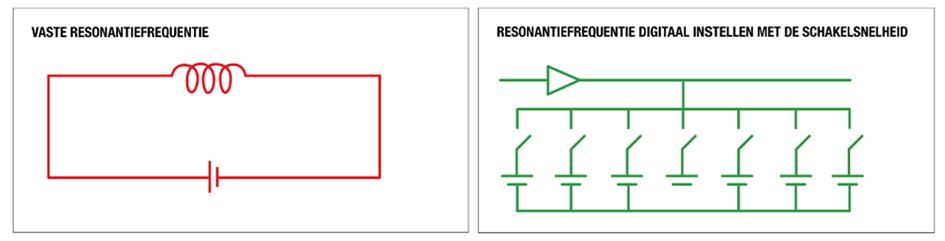
Comparison between Fixed Resonant Frequency and Digital Tuning with N-Path Filters
6. Energy-efficient analog-to-digital converters: The key to IoT
Researchers: Michiel van Elszakker, Simon Louwsma, Ed van Tuyl (†) and Harijot Singh Bindra
In 2010, Michiel van Elszakker, Simon Louwsma, and Ed van Tuyl developed a new analogue-to-digital converter that was not only twenty times more energy-efficient than existing designs but also faster. This record stood for five years. Ten years later, researcher Harijot Singh Bindra brought the world record back to Twente with an even more efficient circuit.
The rise of the Internet of Things (IoT)—a world where countless sensors continuously collect data—makes these innovations crucial. These sensors, often powered by small batteries, need to be extremely energy-efficient. One of the biggest energy consumers is the conversion of physical signals (like temperature, light, or movement) into digital data. This process, called analogue-to-digital conversion, poses a major challenge for IoT applications.
Bindra focused not only on this conversion process, but also on the energy that the sensor continuously consumes to send signals to the converter. Both steps are energy-intensive but often overlooked. Bindra’s design drastically reduces energy consumption for both processes—up to three times more efficient than the most advanced circuits. Energy consumption is now less than one picojoule (one trillionth of a joule) per conversion step.
This improvement means sensors in IoT devices can run for years on a small battery without needing frequent replacements. Bindra’s work contributes to not only better technology but also a more sustainable future where devices use energy more efficiently.
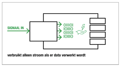
Illustration of an energy-efficient analog-to-digital converter


