Discovering what is inside a three-dimensional (3D) nanostructure, is no longer a matter of cutting slices, thus breaking it up and destroying its functionality. Scientists from the University of Twente and the European Synchrotron Radiation Facilty (ESRF) discovered a new method to look deep inside a 3D nanostructure. This ‘traceless X-ray tomography’ (TXT) can be used for photonics, electron chips and memories, for example. The results are published in the ‘ACS Nano’ journal of the American Chemical Society.
Today, nano-structures are complicated three-dimensional ‘buildings’, for example for manipulating light. Silicon electronics chips, as well, consist of multiple layers of material and interconnecting wires. But how do architects know if the full structure matches their expectations? Looking through a microscope, only the surface can be checked. At this surface level, a ‘good, bad or ugly’ sample may look perfectly the same. One way of looking deeper inside, is cutting the material in this slices and examining those. Of course, it then loses its functionality. The new techniques also creates slices, but these are now 2D images, not physical slices, that together form a 3D image. The structure is fully intact afterwards.
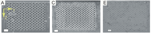
The surfaces of three samples don't show critical differences using microscopy
Over one millimeter
Although X-ray technology has been available for a longer time, it is often still necessary to open up a sample for reaching sufficient depth and contrast. The new traceless X-ray tomography (TXT) makes use of a higher X-ray energy level, thus making it possible to look into samples that have a silicon thickness of over 1 millimeter. The principal author of the ACS Nano paper, Diana Grishina: “In modern nanotechnology this is plenty sufficient to image through wafers. Indeed, all silicon devices remained untouched and ‘as is’ during our study. This is up to 20 times deeper than using existing technologies!” The new method also makes it possible to zoom-in on a desired region.
Higher energy
The X-ray beam, with a photon energy of 17 kilo-electronvolt (keV) is focused to a spot of 23 nanometer by 37 nanometer. These ‘holographic tomography’ experiments were done at the European Synchrotron Radiation Facility (ESRF) in Grenoble, France. The sample is moved and rotated for creating an image at each depth. At the end, intensive processing is done to combine all of these separate image in one 3D image.
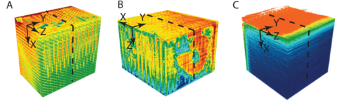
TXT reveals what is really going on, looking inside photonic crystals. 'A' is the only one showing the desired structure. 'B' has a void that will destroy most of the functionality, the pores of 'C' even remain very shallow.
The good, the bad, the ugly
As an example, the researchers took a so-called photonic bandgap crystal, a recent breakthrough in photonics. Its functionality depends on many deep pores in two directions, creating cavities in which light can be manipulated. Although at surface level, the structures seem identical, looking inside reveals that only one of the three is ‘good’. Another has a large void inside due to an error in the manufacturing process: it is ‘bad’. A third one even lacks a 3D structure inside and is ‘ugly’: the pores are too shallow. Leader of the research team, Prof Willem Vos: “TXT serves to non-destructively differentiate between the possible reasons of not finding the designed and expected performance. This is why we think that TXT is an original and powerful tool to critically assess 3D functional nanostructures.”
The research was done in the Complex Photonics Group of UT’s MESA+ Institute, together with the European Synchrotron Radiation Facility in Grenoble, France. It was made possible by the NWO programme ‘Stirring Light’, the Shell/NWO programme ‘Computational Sciences for Energy research’, the Descartes-Huygens Prize of the French Academy of Sciences, and contributions of MESA+ (Applied Nano Photonics) and ESRF (beamtime grants).
The paper ‘X-Ray Imaging of Functional Three-Dimensional Nanostructures on Massive Substrates’, by Diana Grishina, Cornelis Harteveld, Alexandra Pacureanu, D. Devashish, Ad Lagendijk, Peter Cloeten and Willem Vos, will be published in ACS Nano of the American Chemical Society


