M3 Lab: Optoelectronic Materials @ IMS
Our research focusses on the controlled growth and study of novel materials and thin films with functional optical and electrical properties. These materials and thin films find application in state of the art optoelectronic devices such as solar cells, LEDs, transparent electronics, photonics and other energy efficient devices. We work on three main research lines: 1. Vapor-deposited hybrid and inorganic halide perovskites, 2. Transparent conducting oxides (TCOs), 3. P-type transparent material discovery.
Latest news:
- Just out in ACS Materials Letters, our study on the work function of TCO/2 PAC SAMs and the critical role of the TCO microstructures: https://doi.org/10.1021/acsmaterialslett.3c01166. Congrats Suzana!
- Just out in Matter, our work on p-type S-doped CuI transparent conductors. Check it out at: https://doi.org/10.1016/j.matt.2023.10.003. A summary of the work is also available here: https://www.utwente.nl/en/news/2023/11/1219803/creating-efficient-transparent-p-type-conductors. Congrats Adeem!
- PhD candidate Junia Solomon receives a poster prize at the 2023 MRS Spring meeting in San Francisco. Congrats Junia!
- PhD candidate Eloy Marcelis receives a poster prize at the MaterialenNL conference 2023. Congrats Eloy!
- PhD candidate Tatiana Soto Montero received the ‘Best poster award for scientific content’ at the Tandem PV Conference 2022. Congrats Tatiana!
- PI Monica Morales-Masis, featured scientist at UT: https://www.utwente.nl/en/research/researchers/featured-scientists/morales-masis/
- Yury Smirnov received the ‘Best poster award for Scientific Content’ at the Tandem PV Conference 2021.
- Our work has been featured by Coherent, Inc Success Stories. Check it out: https://www.coherent.com/news/success-stories/university-of-twente
Research Projects:
I. Vapor-phase deposited Halide Perovskites: Pulsed (Dual) Laser Deposition as Alternative Technique
CREATE: Crafting Complex Hybrid Materials for Sustainable Energy Conversion (ERC funded project).
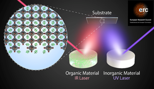
In CREATE we are developing a unique in-vacuum pulsed dual laser deposition (PDLD) method that decouples the deposition of the organic and inorganic sources during growth. This allows the exploration of a full breadth of organic-inorganic halide perovskite compositions and structural motifs, paving the way for discovering new, non-toxic, stable hybrid materials for efficient solar cells, LEDs and beyond.
Pulsed Laser Deposition of Halide Perovskites
Pulsed Laser Deposition (PLD) has offered unique options for the development of complex materials thin film growth, allowing stoichiometric transfer and multi-compound deposition independent of the relative volatility of the elements. We are exploring the potential of PLD as a single-source, solvent free deposition method of halide perovskite thin films.
For more information please check our publications on the topic:
- Single‐Source Vapor‐Deposition of MA1–xFAxPbI3 Perovskite Absorbers for Solar Cells. Adv. Funct. Mater. 2023, 2300588. https://doi.org/10.1002/adfm.202300588
- Pulsed Laser Deposition of Cs2AgBiBr6: from Mechanochemically Synthesized Powders to Dry, Single-Step Deposition. Chem. Mater. 2021, 33, 18, 7417–7422. https://doi.org/10.1021/acs.chemmater.1c02054
- Single-Source, Solvent-Free, Room Temperature Deposition of Black γ-CsSnI3 Films. Adv. Mater. Interfaces, 2020, 7, 2000162. https://doi.org/10.1002/admi.202000162
II. Transparent Conducting Oxides (TCO) for Solar Cells
TCOs are essential in various solar cells, such as silicon heterojunction and perovskite-based solar cells. To allow the maximum amount of sunlight into the cells, the front TCO should be transparent from the UV to the NIR; and to guarantee unhindered carrier extraction, the TCO should have high lateral conductivity and low contact resistance with the adjacent layers of the device. This is a challenge, due to the intrinsic trade-off between transparency and conductivity. Another challenge is the deposition of the TCO without damaging the exposed layers of the solar cells during growth. All these requirements motivate the search for material compositions and synthesis of TCOs, that lead to optimum conductivity and broadband transparency, for example by achieving high electron mobilities, while avoiding damage to the device by performing a gentle, soft-landing deposition. One of the techniques we are exploring for this is pulsed-laser deposition (PLD). Materials we are currently studying include zirconium-doped indium oxide (In2O3:Zr), tin-doped indium oxide (ITO), tantalum-doped tin oxide (SnO2:Ta) and lanthanum-doped barium tin oxide (LBSO).
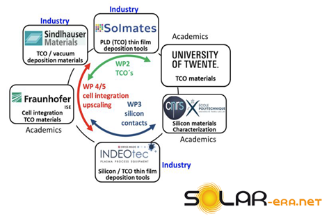
- Solar ERA NET funded project: Cost efficient, upscalable and stable transparent conductive oxides for silicon solar cells based on passivated contacts (CUSTCO).
Main publications on TCOs:
- Impact of the TCO Microstructure on the Electronic Properties of Carbazole-Based Self-Assembled Monolayers . ACS Materials Lett. 6 (2024). https://doi.org/10.1021/acsmaterialslett.3c01166
- Wafer-Scale Pulsed Laser Deposition of ITO for Solar Cells: Reduced Damage vs Interfacial Resistance. Materials Advances, (2022). https://doi.org/10.1039/D1MA01225H
- Scalable Pulsed Laser Deposition of Transparent Rear Electrode for Perovskite Solar Cells. Adv. Mater. Technol., 6, 2, 2000856 (2021). https://doi.org/10.1002/admt.202000856
- Sputtered transparent electrodes for optoelectronic devices: Induced damage and mitigation strategies. Matter, 4 (11), (2021). https://doi.org/10.1016/j.matt.2021.09.021
- Origins of infrared transparency in highly conductive perovskite stannate BaSnO3, APL Materials, (2020)
- Transparent Electrodes for Efficient Optoelectronics. Adv. Electron. Mater. Vol. 3 (2017). https://doi.org/10.1002/aelm.201600529
III. P-type Transparent Material Discovery
NWO Start-Up funded project: Bridging the p-type transparent materials discovery gap (BRIDGE).
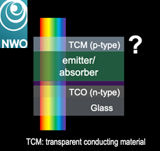
Most TCOs and semiconducting oxides known to date are n-type. The challenge for p-type conductivity in oxides originates from a highly-localized oxygen 2p valence band (low hole mobilities) and the positioning of the valence band well below the vacuum level (high ionization potentials). Recent computational predictions propose strategies to achieve valence band delocalization, lowering the hole effective mass and increasing hole mobility. We are exploring these hypothesis by synthesizing the materials and characterizing the optoelectronic and compositional properties to determine the most promising compositions for p-type transparent materials and optimize them for application as p-type contacts in solar cells.
Main publications on p-type TCMs:
- The role of sulfur in sulfur-doped copper(I) iodide p-type transparent conductors. Matter, 6 (2023). https://doi.org/10.1016/j.matt.2023.10.003
- Bridging the p-type transparent conductive materials gap: synthesis approaches for disperse valence band materials. J. of Photonics for Energy, 10 (4) (2020). https://doi.org/10.1117/1.JPE.10.042002
The team
PI
- Dr. Monica Morales-Masis (Associate Professor) (https://personen.utwente.nl/m.moralesmasis)
PhD candidates
- Tatiana Soto-Montero (https://personen.utwente.nl/t.d.s.sotomontero)
- Adeem Mirza (https://personen.utwente.nl/a.s.mirza)
- Junia Solomon (https://personen.utwente.nl/j.s.s.solomonsathiaraj)
- Suzana Kralj (https://personen.utwente.nl/s.k.kralj)
- Eloy Marcelis (https://people.utwente.nl/e.j.marcelis)
Postdocs
- Paul Llontop
- Wiria Soltanpoor (https://personen.utwente.nl/w.soltanpoor)
Master students
- Vojta Kliner
- Marly Nales (AP)
Student Assistant
- Ivaylo Lazarov (CSE)
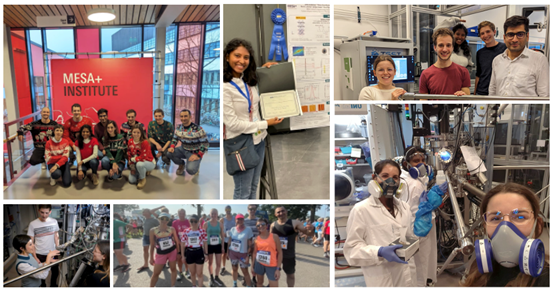
Figure 1. Team members, 2023-2024.
Alumni:
- Dr. Yury Smirnov (https://www.linkedin.com/in/yurysmirnov/)
- Dr. Pierre-Alexis Repecaud
IV. Funding

- ERC StG 2019 – Project CREATE
- ERC PoC 2022 – Project SPRINT
- NW0 Start-Up Grant 2019 – Project BRIDGE
- CETPartnership and NWO – Project EPoBoC
- SOLAR ERA-NET 2019 – Project CUSTCO
V. Publications (links)
https://orcid.org/0000-0003-0390-6839
VI. Media
Follow us on:
Twitter: @m3lab_ (link: https://twitter.com/m3lab)