 In this thesis one of the main drawbacks of polymer waveguides for optical applications was addressed: the typically low refractive index, making them disadvantageous in offering sharp bent waveguides, causing high bend losses.
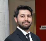
‘First, we numerically calculated a metal layer underneath the core of a polymer waveguide,’ Mustafa Akin Sefunc says. ‘It proved that sharp bends are realisable, and the reduction of bend losses substantial. From there we presented the design, fabrication and characterization of such waveguides. We have shown that embodying a metal layer, is beneficial for the reduction of losses in sharp bent waveguides.’
In the second part of the thesis, the attention was on waveguide amplifiers. First the focus was on developing fabrication techniques – crystal bonding and thinning- for the realization of high-index-contrast waveguide architecture. For example, focused ion beam milling was utilized for patterning the waveguides, and also a fabrication process based on argon plasma etching has been developed.
‘This work was part of a STW-call project,’ Mustafa says. ‘Several companies were involved, such as: UT spin-off companies Lionix and PhoeniX Software, as well as TNO, TE Connectivity and IBM Zürich. The half-yearly meetings were very inspiring. Using our fabrication methods one can integrate the newly fabricated components and integrate them, to really change waveguide architectures.’
Halfway the PhD project Mustafa was rewarded an internationally highly renowned SPIE Optics and Photonics Education Scholarship award. ‘As the only laureate from the Netherlands, this reward meant a lot to our approach within the Optical Sciences (OS) Group,’ Mustafa says.

The kind of concept demonstrations can be positioned between fundamental research and application driven research, Mustafa believes. ‘I value this special stage as a decisive one, as without learning to control new fabrication techniques, no valuable novelties can be created at all. An important step towards feasible future application, for example, was our successful use of argon plasma etching (instead of focused ion beam milling, which is more costly), opening ways to fabricate novel kind of future waveguides in higher numbers.’
Ongoing research
Mustafa is happy he contributed to an ongoing line of research of the OS Group, as Associate Professor Sonia Garcia-Blanco succeeded in bringing in an European Research Council (ERC) grant on this topic. Three new PhD researchers will continue this line of research now.

‘Because of the SPIE reward I was happy to be a speaker on as much as six conferences all over the world,’ Mustafa says. ‘Especially memorable were the IEEE Photonics Society Benelux meetings. In 2014 I helped organizing the edition taking place at the University of Twente, hosting around 140 researchers in the field.’
Nanolab
Working around 380 hours in the Mesa+ Nanolab, Mustafa appreciated greatly. ‘The years-long experience of the technicians is irreplaceable in this respect,’ he says. ‘The cleanroom is run as a company in itself, hosting most up-to-date equipment, making it well-planned and widely available for all PhD researchers.’

‘The technicians were guiding me, correcting fabrication recipes in an early stage, if there was reason to do so. At the same time I had great flexibility in finding my own route towards exploring new paths of research. That is a special combination Mesa+ is offering.’
Future career
Continuing his career in industry is appealing to Mustafa, favourably at a small start-up company situated in Enschede.
‘I prefer a flat organisation structure, working flexible, everybody helping each other out while working on innovations. This atmosphere I met at our Active NanoPhotonics group as well. During the monthly meetings we learned from presenting our work to one another. The atmosphere was truly confidential, allowing us to speak up and comment the work of the members in a fair manner, alsogiving room to criticism. One can benefit from that greatly.’
