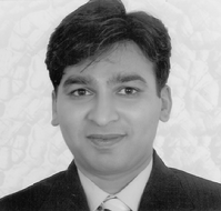
Capacitively transduced polycrystalline GeSi MEM resonators
Promotion date: June 18.
Promotor: Prof.dr. Jurriaan Schmitz
Assistant Promotor: Dr.ir. Cora Salm
| Wireless communication systems rely on their ability to select or generate signals with a very precise frequency. The common feature of filters and oscillators, is their use of resonators. The contemporary wireless systems, nowadays, utilize off–chip components that occupy large space at board level and consume substantial amounts of power. Bulk mode MEM resonators are emerging as the prime candidates for being used as frequency selection and generation components, due to their ability to resonate at GHz frequencies and their exceptionally high quality factors. They are envisioned to replace the existing off–chip components with on–chip micromachined counterparts. The above-IC integration of micromechanical components on top of CMOS chips can potentially leads to miniaturized low–power, low cost, and high–performance wireless communication systems on a single chip. The objective of this research is to apply CMOS post–processing compatible material to fabricate bulk mode MEM resonators that can be used for filtering and oscillator functions in wireless front–end architectures. This research provides a proof of principle that MEM resonators can be fabricated with exceptionally high quality factors using low stress and highly conductive poly Ge0.7Si0.3 structural layers. The motional resistance is still high for the fabricated devices (that mostly limits their use for filtering applications). They can potentially replace the quartz crystals used for local oscillators. |
Was your work application oriented or were also fundamental issues involved?
The main approach was application oriented, aimed at replacing SAW, ceramic filters and crystal based oscillators by MEM filters and oscillators for low power, low cost and above-IC integration wireless communication systems. Tailoring stress, resistivity and highly anisotropic etching of the structural layers, are the challenging parameters to deal with. Also Borrom doping appears to be an important way to control resistivity and stress in the structural layers.
My research was on tiny things able to perform heavy work. Fundamental aspects for these future bulk materials are mostly found in literature. The equipment for experimenting on them is available at the MESA+ Test Centre. As a member of the STW funded project; CMOS Receiver Enhancement using Array with MEMS (CREAM), I closely collaborated with the Integrated Circuit Design Group and the Transducer Science & Technology Group. It was a nice challenge to investigate this new approach towards filter and oscillator replacements for future applications.
In what way did you develop as a researcher and scientist during this PhD period?
In the first phase of the project I learned many aspects on micro fabricating skills by the courses I attended.
More in general: I learned to work much more systematically as before. A systematical approach is needed, especially in nano research, as the experiment equipment is very costly as are the samples one works with. You have to prepare and schedule all aspects well-ahead, knowing what to do in all stages of research.
In reading and studying literature, I evolved a great deal. Now I am able to find the essence of publications much quicker, not going into details too much, pinpointing the main results efficiently.
In presentation I improved a lot: communicating better with colleagues and scientists from abroad. Also I attended three conferences, doing oral and poster presentations.
Do you recall some special moments?
During the first year I can recall some targets were set within a short period of time. I succeeded in coming through this period well, which was a good thing for my confidence. After that I knew I could cope with the new skills learned.
Also I remember a STW meeting. Here I presented a high-Q resonator which I fabricated the evening just before the meeting. I wasn’t able to do extensive testing for this practical demonstration, for example how tuning would vary as voltages were changed. Although this was somehow stressful, the results proved out to be very good that day.
Did you have some nice articles published?
Two papers were published, in Electrochemical Society and Microelectronic Engineering. One article is under preparation still.
Also I had the honor of presenting our work at the IEEE International Frequency Control Symposium(IFCS)2012. Here I was selected amongst the finalists for best student paper competition.
What are your future plans?
At the moment I am working at the National Institute of Laser and Optronics in my home country Pakistan. I am happy being able to stay in academics as this work involves all kinds of aspects, whereas industrial research is more specialized. Also the international contacts, and meeting new people in the field of communication, microfluids, fabrication and experimentation experts, is very appealing to me.
The job I am working on is very similar to the PhD work. Here in Pakistan we possess some nice equipment apparatus. The comparison to Mesa+ is not possible. We need at least twenty more years of progress.
Having experimental skills is a big advantage in Pakistan. I am able to introduce microfabrication skills as I have experienced hands-on skills during my PhD project. Most scientists here are theoretical and simulation experts.
Did you feel member of the Mesa+ family while working on your PhD thesis?
Mesa+ was among the very first things I learned to know in the Netherlands, and I felt at home here straightaway. The culture here is very open. All colleagues were more than willing to help me out when help or support was needed. This highly progressive working atmosphere is a big strength of Mesa+.
I guess, still more collaboration between groups is feasible within Mesa+. New connections will enable groups to specialize on new, emergent research topics.

