All-Optical Processes in Integrated Optical Devices Utilizing Materials with Large Third Order Nonlinearities and Gain
Promotion Date: 22 December 2006
| Light plays an ever-increasing important role in the field of data communication. Modern data communication is nothing but light pulses propagating through a glass fibre cable. The capacity for data transfer in a glass fibre is enormous; even such that half of the world’s population could have a telephone conversation with the other half simultaneously, through one single fibre. But a bottleneck occurs in places where the light has to be routed to reach the end user (the light has to change its direction) for which purpose the light signal is converted into an electrical signal. I worked on the development of a chip that can switch the direction of the light all-optical, i.e. the light pulse is not converted into an electrical signal. |
What was your thesis about?
Light plays an ever-increasing important role in the field of data communication. Modern data communication is nothing but light pulses propagating through a glass fibre cable.
The capacity for data transfer in a glass fibre is enormous; even such that half of the world’s population could have a telephone conversation with the other half simultaneously, through one single fibre. But a bottleneck occurs in places where the light has to be routed to reach the end user (the light has to change its direction) for which purpose the light signal is converted into an electrical signal. I worked on the development of a chip that can switch the direction of the light all-optical, i.e. the light pulse is not converted into an electrical signal.
It sounds like a breakthrough, how did you do it?
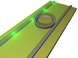
Typically, the light is confined in a straight waveguide. On the chip there are two of such parallel waveguides, connected in the middle by a ring. Through one of the waveguides a laser pulse (green) is inserted of which a bit of the light leaks into the ring. Depending on the size of the ring, certain colours (red, in this case) will be transferred to the second channel.
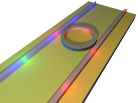
By using an extra pulse (blue), the colour of the light can be changed, for instance from green to red. This way you could build an optical transistor as follows: without an extra pulse the light travels straight through the first channel and represents a ‘0’ and with a pulse the light travels through the ring to the parallel channel resulting in a ‘1’.
|
|
How far is this off from a real device?
We have spent a lot of time looking into different materials to use for this kind of chip and even studied the wildly exotic ones with highly nonlinear properties. Exploiting the optical nonlinearity of an optical device still needs a great deal of investigation and it will take another five years at least before we can come up with something that also has industrial promise.
And the outcome of your material research?
It seems that the results with silicon, quite a straightforward material, are the best after all.
What did you like best about your research?
The fact that you yourself are fully responsible for the way you carry out the research. Furthermore, I had the opportunity to study this problem from many angles, testing all the different materials.
Did you experience any setbacks in your research?
Well, the versatility of the research into which material to use might also be looked upon as a problem because of the many uncertain outcomes, but I always had my backup plans.
There was a material that was very difficult to etch and we did not have the proper equipment to do so. Therefore, I switched to polymer based materials in which you can make structures with UV light.
Have you always been interested in optics?
I was always more or less involved with optics. After I graduated from Technical College (HTS), I planned to study Applied Physics at this university. In order to fill the time gap between my graduation and the start of the academic year, I started a job in the clean room as a clean room technician. I stayed on that job for three years. Then I moved to Arnhem to work with a telecom company called JDS Uniphase. That was just before the telecom bubble burst. After 1.5 years I went to Canada to work for that same company. I stayed there for another 1.5 year, but then the bubble definitely burst and the numbers of staff fell from 11,000 to less than 1,000. I lost my job as well and decided that I wanted to do a PhD next.
Usually that is difficult without a Master’s degree, but because of my job experience I qualified for this project. In the first year I took up some extra lectures to catch up on the theory.
What about your future?
First I will pursue a post-doc position in our group and after that… I am not sure.
I am interested in working for a spin-off to commercialize integrated optical devices.
But before we can start on that, we have to look into the feasibilities in a bit more detail.